STIL04-P5(2002) Ver la hoja de datos (PDF) - STMicroelectronics
Número de pieza
componentes Descripción
Fabricante
STIL04-P5 Datasheet PDF : 7 Pages
| |||
STIL04-P5
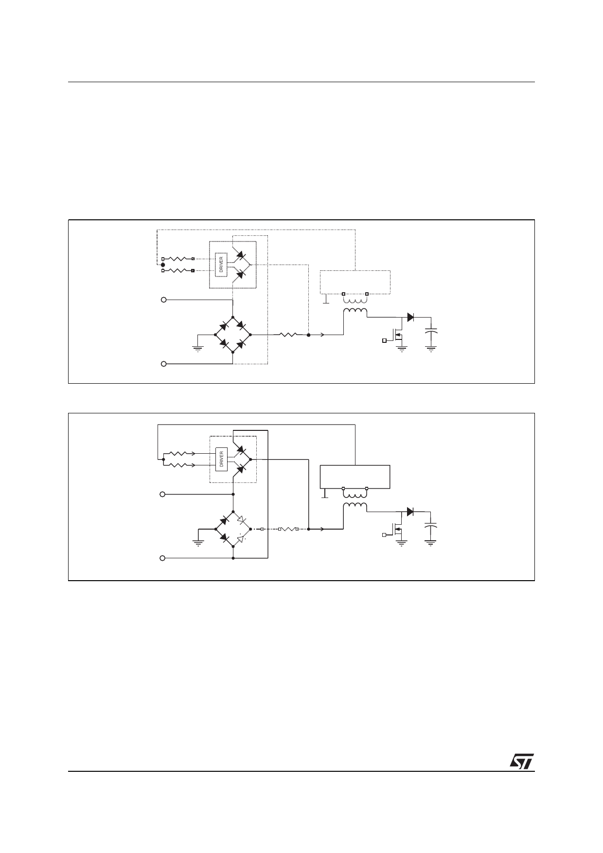
Functional Description
The STIL04 is connected in parallel with the bridge diode and the inrush power resistor Ri (fig. A2). During
start up, the two unidirectional ASD™ power switches of the STIL04 are opened. The inrush current flows
through the diodes of the bridge and the external inrush power resistor Ri. Since the main converter turns
ON, the auxiliary power supply coupled with the main transformer, supplies the energy required to close
the two power switches of the STIL04. At the normal state, the two bottom diodes of the bridge rectifier and
the two unidirectional switches of the STIL04 rectify the AC line current.
When the STIL04 is used with a PFC boost converter, the inrush current circuit remains active after a short
AC line dropout (see fig. A5). In that configuration, since the AC line disappears, the PFC controller and the
auxiliary power supply of the STIL turns OFF. The two switches of the STIL are opened. The output bulk
capacitor Cb is discharging and it is providing the energy to the main converter. When the AC line recovers,
the two switches remain opened and recharging inrush current of the capacitor Cb is deviated and limited
through the resistor Ri. When the capacitor is charged, the PFC turns ON again and the two switches of the
STIL switch ON.
More details on the design and operation of the driver circuit of figure A5 can be found in the application
note “AN1600 - STIL: Inrush Current Limitation Device for Off-Line Power Converter”.
ABSOLUTE MAXIMUM RATINGS (Limiting value)
Symbol
Parameter
VDout
VRout
Iout(AV)
Repetitive forward (VDout) and reverse (VRout)
off-state voltage
Average on state current at the OUT terminal
(180° conduction angle for the internal power
switches)
Iout(RMS) RMS on state current at the OUT terminal
(180° conduction angle for the internal power
switches)
ITSM Non repetitive surge peak on-state current
(Tj initial = 25°C)
I2t
I2t value - rating for fusing
dIout/dt Critical rate of rise of on state current
Ipt1 + Ipt2 = 20mA
Tstg Storage temperature range
Tj
Junction temperature range
Tj (min) to
Tj (max)
Tj = 150°C
Value
700
4
Tj = 150°C
4.4
tp = 10ms
sinusoidal
tp = 10ms
Tj = 25°C
Tj = 150°C
65
21
100
-40 to +150
0 to +150
Unit
V
A
A
A
A2s
A/µs
°C
°C
THERMAL PARAMETERS
Symbol
Parameter
Rth(j-c)
Rth(j-a)
Junction to case
Junction to ambient (minimum footprint)
Value
2
60
Unit
°C/W
2/7
Share Link: 