SIP1759 Ver la hoja de datos (PDF) - Vishay Semiconductors
Número de pieza
componentes Descripción
Fabricante
SIP1759 Datasheet PDF : 8 Pages
| |||
SiP1759
Vishay Siliconix
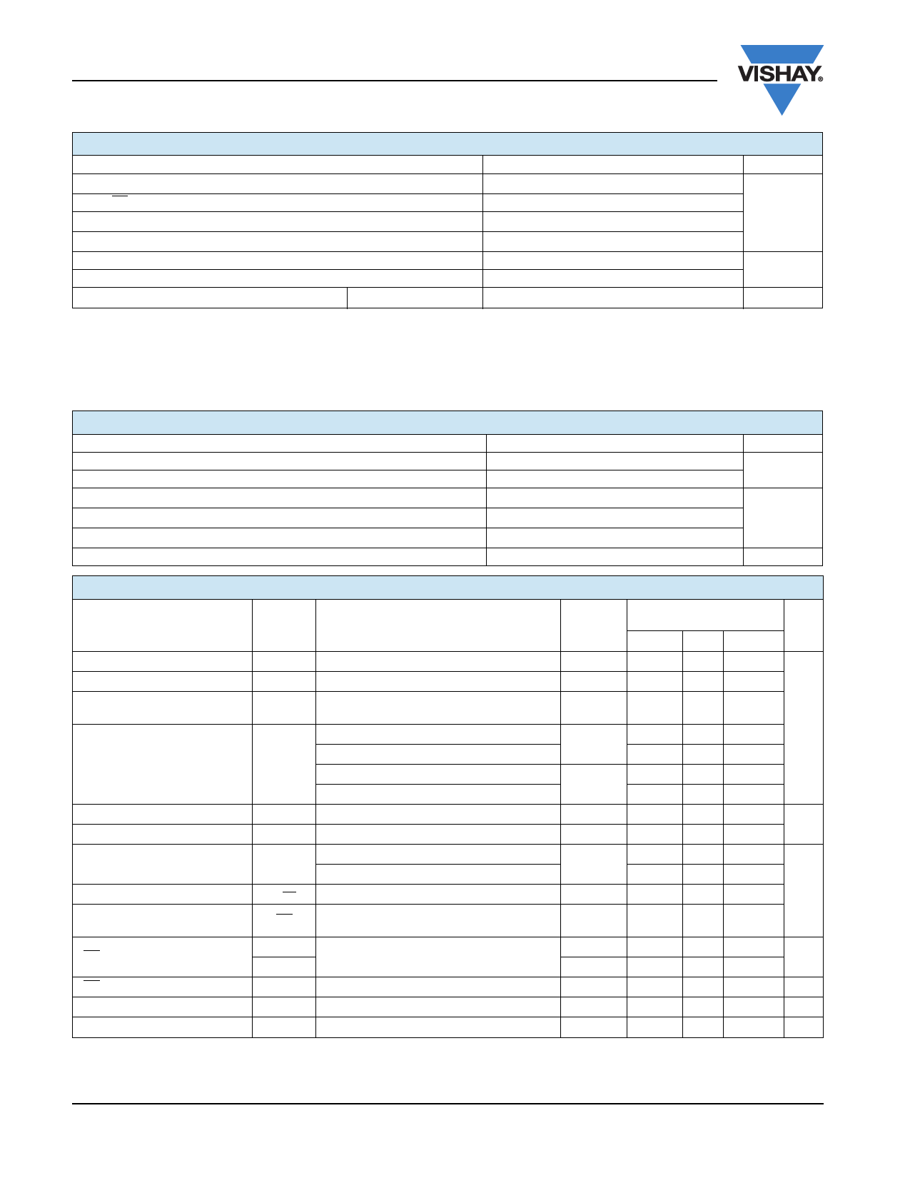
ABSOLUTE MAXIMUM RATINGS (all voltages referenced to GND = 0 V)
Parameter
Limit
Unit
Input Voltage (VIN)
OUT SD, FB, ERROR to GND
CX- to GND
CX+ to GND
Storage Temperature
Maximum Junction Temperature
- 0.3 to 6
- 0.3 to 6
- 0.3 to (VIN + 0.3)
V
- 0.3 to (the greater of VIN or VOUT) + 1)
- 55 to 150
°C
150
Power Dissipationa,b
MSOP-10 (TA = 70 °C)
444
mW
Notes:
a. Device Mounted with all leads soldered or welded to PC board.
b. Derate 5.6 mW/°C above 25 °C.
Stresses beyond those listed under “Absolute Maximum Ratings” may cause permanent damage to the device. These are stress ratings only, and functional operation
of the device at these or any other conditions beyond those indicated in the operational sections of the specifications is not implied. Exposure to absolute maximum
rating conditions for extended periods may affect device reliability.
RECOMMENDED OPERATING RANGE (all voltages referenced to GND = 0 V)
Parameter
Limit
Unit
Input Voltage Range
Output Voltage Adjustment Range
1.6 to 5.5
V
2.5 to 5.5
CIN
CX
COUT
Operating Temperature Range
10
0.33
µF
10
- 40 to 85
°C
SPECIFICATIONS
Parameter
Input Voltage Range
Input Undervoltage Lockout
Output Voltage Adjustment
Range
Output Voltage
Maximum Output Current
Transient Load Current
Quiescent Supply Current
Shutdown Supply Current
Output Leakage Current in
Shutdown
SD Logic Input Voltage
SD Input Leakage Current
FB Regulation Voltage
FB Input Current
Symbol
VIN
VUVLO
VOUT
IOUT(max)
IQ
IQSD
SD
VIL
VIH
VFB
IIFB
Test Condition Unless Specified
VIN = VSD = 2 V, FB = PGND = GND
CIN = 10 µF, Cx = 0.33 µF, COUT = 10 µF
Temp.a
Full
Full
Limits
- 40 °C to 85 °C
Min. Typ.b Max. Unit
1.6
5.5
0.7
1.0
1.5
1.6 V ≤ VIN ≤ 5.5 V
Full
2.5
5.5
2 V ≤ VIN ≤ 5.5 V, 1 mA ≤ IOUT ≤ 50 mA
0 °C to
3.17 3.3
3.43
V
2.5 V ≤ VIN ≤ 5.5 V, 1 mA ≤ IOUT ≤ 100 mA
85 °C
3.17 3.3
3.43
2 V ≤ VIN ≤ 5.5 V, 1 mA ≤ IOUT ≤ 50 mA
Full
2.5 V≤ VIN ≤ 5.5 V, 1 mA ≤ IOUT ≤ 100 mA
3.15
3.15
3.45
3.45
2.5 V ≤ VIN ≤ 5.5 V
Full
100
mA
IOUT ≤ 100 mA (RMS)
0 °C to 85 °C
200
VIN = VSD = 4 V, VFB = 0 V, Stepping Down
Full
VIN = VSD = 2 V, VFB = 0 V, Stepping Up
1.6 V ≤ VIN ≤ 5.5 V, VSD = 0 V
Full
60
100
60
100
1
5
µA
VIN = 2 V, VOUT = 3.3 V, VSD = 0 V
Full
1
5
1 6 V ≤ VIN ≤ 5 5 V
VSD = 5.5 V
VIN = 1.65 V, VOUT = 3.3 V
VFB = 1.27 V
Full
Full
0.7 * VIN
0.25 * VIN
V
Full
-1
1
µA
Full
1.205 1.235 1.265
V
Full
25
200
nA
www.vishay.com
2
Document Number: 72949
S09-1453-Rev. D, 03-Aug-09
Share Link: 