SG6741A Ver la hoja de datos (PDF) - Fairchild Semiconductor
Número de pieza
componentes Descripción
Fabricante
SG6741A Datasheet PDF : 12 Pages
| |||
Marking Information
SG6741ATP
XXXXXXXXYWWV
※marking for SG6741ASZ
ZXYTT
6741A
TPM
※marking for SG6741ASY
T: S = SOP
P: Z =Lead Free
Null=regular package
XXXXXXXX: Wafer Lot
Y: Year; WW: Week
V: Assembly Location
F: Fairchild logo
Z: Plant code
X: 1 digit year code
Y: 1 digit week code
TT: 2 digits die run code
T: Package type (S = SOP)
P: Y=Green package
M: Manufacture flow code
Figure 3. Top Mark
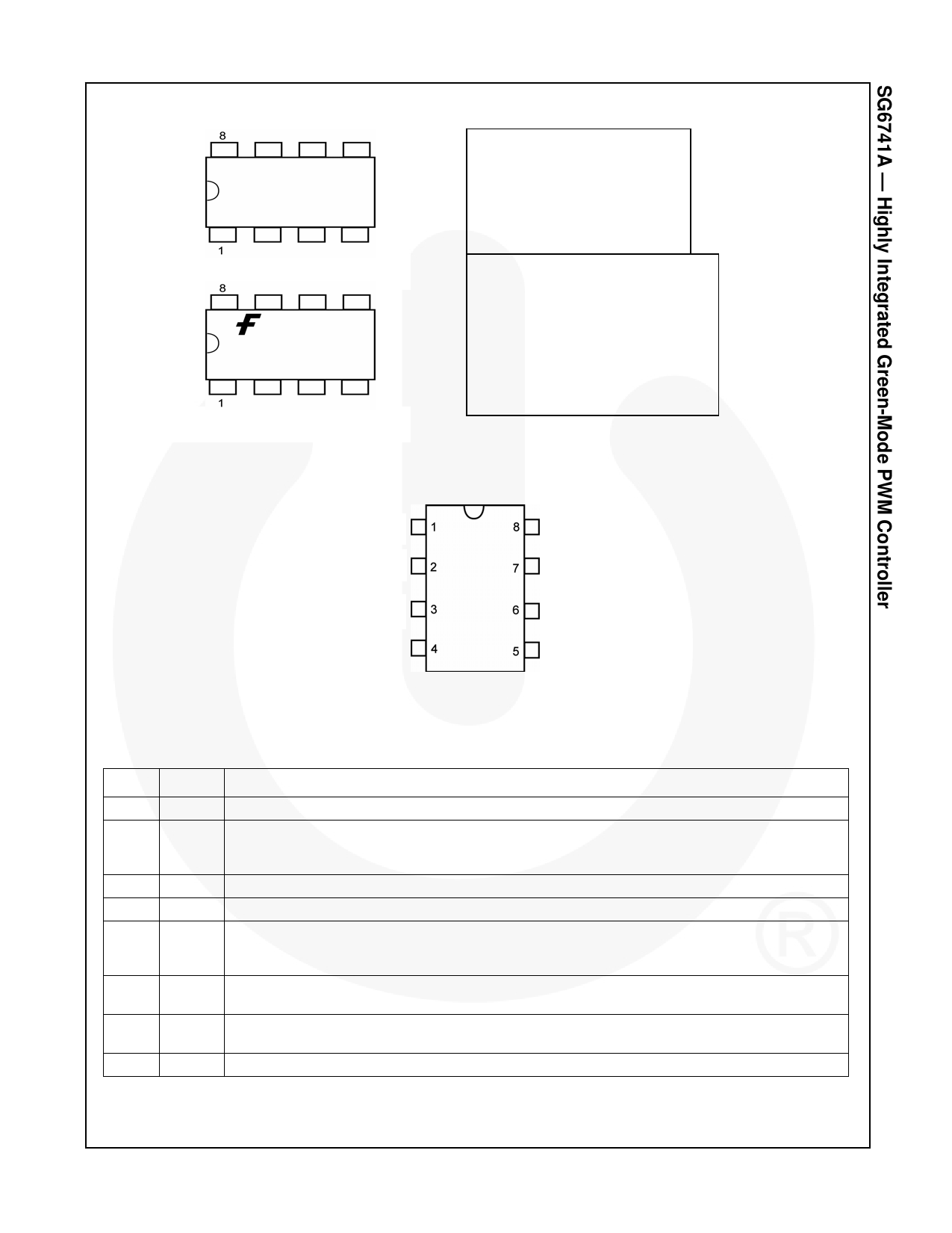
Pin Configuration
GND
FB
NC
HV
GATE
VDD
SENSE
RI
Figure 4. Pin Configuration
Pin Definitions
Pin #
1
2
3
4
5
6
7
8
Name
GND
FB
NC
HV
RI
SENSE
VDD
GATE
Description
Ground.
Feedback. The signal from the external compensation circuit is fed into this pin. The PWM duty
cycle is determined in response to the signal on this pin and the current-sense signal on SENSE
pin.
No Connection.
Startup Input. For startup, this pin is pulled HIGH to the line input or bulk capacitor via resistors.
Reference Setting. A resistor connected from the RI pin to GND pin provides a constant current
source, which determines the center PWM frequency. Increasing the resistance reduces PWM
frequency. Using a 26KΩ resistor for RI results in a 65kHz center PWM frequency.
Current Sense. The sensed voltage is used for peak-current-mode control and cycle-by-cycle
current limiting.
Power Supply. The internal protection circuit disables PWM output as long as VDD exceeds the
OVP trigger point.
Driver Output. Totem-pole output driver. Soft driving waveform is implemented for improved EMI.
© 2008 Fairchild Semiconductor Corporation
SG6741A • Rev. 1.0.1
3
www.fairchildsemi.com
Share Link: 