SG2540M Ver la hoja de datos (PDF) - Microsemi Corporation
Número de pieza
componentes Descripción
Fabricante
SG2540M Datasheet PDF : 6 Pages
| |||
APPLICATION INFORMATION
SG1540/SG2540/SG3540
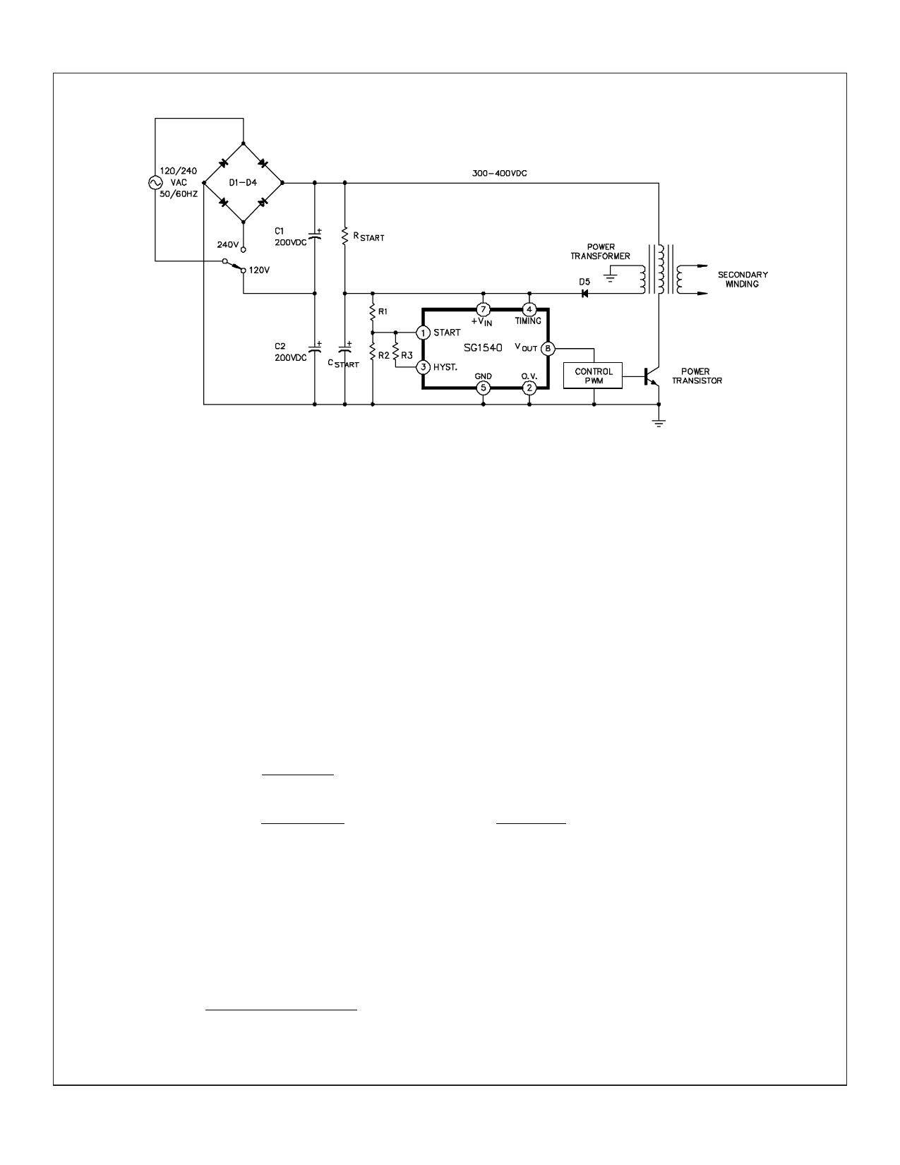
FIGURE 3 - EFFICIENT PRIMARY SIDE START-UP
PRIMARY SIDE START-UP
When the design goal is efficient start-up for a control PWM referenced to the primary side of the power transformer, the configuration
in Figure 3 is recommended. An energy storage capacitor CSTART is trickle-charged from the 300-400 Volt DC bus by resistor RSTART.
The value of RSTART is chosen to provide a constant 1mA charging current, allowing the use of a ½ watt resistor. As the voltage on
CSTART ramps up from zero, the only load current is the standby current of the SG1540 and that of the divider network R1-R3. (Connecting
the TIMING pin to +VIN disables the internal power oscillator and forces the circuitry into a micropower standby model. Since the input
bias current at the START pin is 1µA maximum, a divider current of 100µA is adequate).
When the voltage at the START pin reaches +2.5 Volts, the hysteresis transistor turns off, overdriving the START pin. The VOUT pin
is switched to the HIGH state, providing power to the PWM control circuit. As energy flows out of the START capacitor, its voltage
decays; but it remains connected to the PWM circuit until the dropout voltage is reached (VSTART - VHYSTERESIS). The bootstrap winding
on the power transformer and rectifier diode D5 prevent this from happening. As the PWM control circuit becomes active, the power
transistor begins to switch, providing operating current to the PWM circuit through the SG1540.
RESISTOR CALCULATIONS
Given that VSTART and VDROPOUT have been chosen, and that the divider current at start-up is 100µA, then the values for R1 through R3
are calculated as follows:
1. For simplification, let X = VSTART - 2.5
2.5
and Y = VDROPOUT -2.5
2.5
2. Then,R1 = 2.5 x 10⁴ * X
[1]
R2 = R1/Y
[2]
and R3 = R1 * R2
[3]
X * R2 - R1
DESIGN EXAMPLE
Suppose we have a power MOSFET device, and so want to start at +18 volts and drop out at +12 volts.
Then
X = 6.20
and Y = 3.80
Therefore
R1 = 2.5 x 104 * 6.2 = 155K
R2 = 1.5 x 10⁵/3.8 = 39.5K
R3 = 1.5 x 105 * 3.9 x 104 = 63.7K
6.2 * 3.9 x 104 - 1.5 x 10⁵
(Choose 150K)
(Choose 39K)
(Choose 62K)
4/90 Rev 1.1 2/94
Copyright © 1994
LINFINITY Microelectronics Inc.
4
11861 Western Avenue ∞ Garden Grove, CA 92841
(714) 898-8121 ∞ FAX: (714) 893-2570
Share Link: 