SG1532T Ver la hoja de datos (PDF) - Microsemi Corporation
Número de pieza
componentes Descripción
Fabricante
SG1532T Datasheet PDF : 5 Pages
| |||
SG1532/SG2532/SG3532
ABSOLUTE MAXIMUM RATINGS (Note 1)
Pulse (50 ms) Input Voltage from V to V- .......................
IN
50V
Continuous Input Voltage from VIN to V-............................ 40V
Input to Output Voltage Differential................................... 40V
Maximum Output Current ........................................... 250mA
Current from VZ (J, L-Package only)............................. 100mA
Note 1. Exceeding these ratings could cause damage to the device.
Current from V ..........................................................
REF
25mA
Operating Junction Temperature
Hermetic (T, J, L-Packages)....................................... 150°C
Storage Temperature Range .......................... -65°C to 150°C
Lead Temperature (Soldering, 10 Seconds) ................. 300°C
THERMAL DATA
J Package:
Thermal Resistance-Junction to Case, θJC .................. 30°C/W
Thermal Resistance-Junction to Ambient, θJA .............. 80°C/W
T Package:
Thermal Resistance-Junction to Case, θJC .................. 25°C/W
Thermal Resistance-Junction to Ambient, θJA ........... 130°C/W
L Package:
Thermal Resistance-Junction to Case, θJC .................. 35°C/W
Thermal Resistance-Junction to Ambient, θJA ........... 120°C/W
Note A. Junction Temperature Calculation: TJ = TA + (PD x θJA).
Note B. The above numbers for θJC are maximums for the limiting
thermal resistance of the package in a standard mount-
ing configuration. The θJA numbers are meant to be
guidelines for the thermal performance of the device/pc-
board system. All of the above assume no ambient
airflow.
RECOMMENDED OPERATING CONDITIONS (Note 2)
Input Voltage Range
SG1532/SG2532 ................................................. 5V to 45V
SG3532 .............................................................. 5V to 36V
Output Current Range ....................................... 1mA to 100mA
Note 2. Range over which the device is functional.
Reference Current ........................................................ 5mA
Zener Current (J & L-Packages only) ........................... 20mA
Operating Ambient Temperature Range
SG1532 ........................................................ -55°C to 125°C
SG2532/SG3532 .............................................. 0°C to 70°C
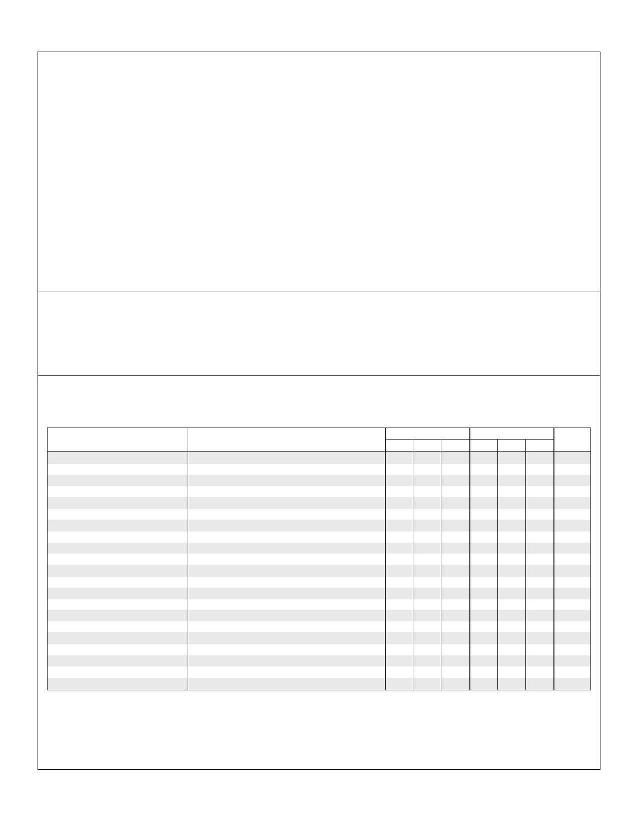
ELECTRICAL CHARACTERISTICS
(Unless
otherwise
specified,
these
specifications
apply
over
the
operating
ambient
temperatures
for
SG1532
with
-55°C
≤
T
A
≤
125°C,
SG2532
with
0°C ≤ TA ≤ 70°C, SG3532 with 0°C≤ TA ≤ 70°C, VIN = 10V, VOUT = 5V, and IOUT = 1mA. Low duty cycle pulse testing techniques are used which maintains
junction and case temperatures equal to the ambient temperature.)
Parameter
Test Conditions
SG1532/SG2532
SG3532
Units
Min. Typ. Max. Min. Typ. Max.
Input Voltage Range
TA = 25°C
4.5
50 4.5
40
V
4.7
50 4.7
40
V
Output Voltage Range
Max Output Current
Min (VIN - VOUT)
Reference Voltage
RSC = 0, VOUT = 0, TA = 25°C
IOUT = 100mA, TA = 25°C
TA = 25°C
2.0
38 2.0
38
V
175 250
175 250 mA
1.7 2.0
1.7 2.0 V
2.40 2.50 2.60 2.40 2.50 2.60 V
2.35
2.65 2.35
2.65 V
Temperature Stability (Note 4)
Ref Short Circuit Current
Line Regulation (Note 3)
Load Regulation (Note 3)
Current Limit Sense Voltage
Shutdown Voltage Threshold
Shutdown Source Current
Zener Voltage
Standby Current
Error Amplifier Offset Voltage
VREF = 0, TA = 25°C
8V ≤ VIN ≤ 40V
8V ≤ VIN ≤ 20V, IOUT = 25mA
1mA ≤ IOUT ≤ 25mA
1mA ≤ IOUT ≤ 100mA
RSC = 100Ω, VOUT = 0V
VOUT = high
IOUT = 10mA, (J and L-Packages only)
VIN = 40V
0.005 0.015
15 25
0.005 0.01
0.01 0.02
0.002 0.004
0.002 0.005
0.06 0.08 0.10 0.06
0.40 0.70 1.0 0.40
100 200 300 100
6.0 6.4 7.2 6.0
2.5 3.5
2.0 10
0.005 0.015
15 25
0.005 0.02
0.01 0.03
0.002 0.004
0.002 0.005
0.08 0.10
0.70 1.0
200 300
6.4 7.2
2.5 3.5
2.0 15
%/°C
mA
%/V
%/V
%/mA
%/mA
V
V
µA
V
mA
mV
Error Amplifier Input Bias
Current
4.0 15
4.0 20 µA
2/93 Rev 1.1 2/94
Copyright © 1994
LINFINITY Microelectronics Inc.
2
11861 Western Avenue ∞ Garden Grove, CA 92841
(714) 898-8121 ∞ FAX: (714) 893-2570
Share Link: 