MRFIC0914 Ver la hoja de datos (PDF) - Motorola => Freescale
Número de pieza
componentes Descripción
Fabricante
MRFIC0914 Datasheet PDF : 6 Pages
| |||
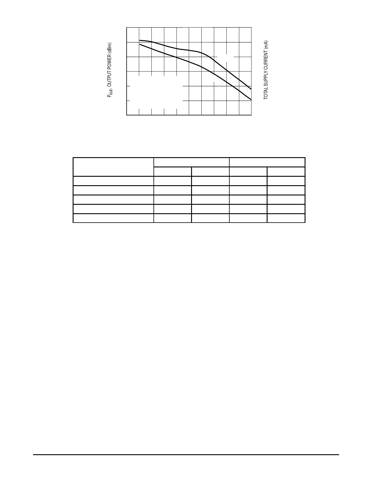
30.75
620
30.50
IDtotal
600
TA = 25°C
Pout
30.25 f = 900 MHz
VCNTRL = 4 V, 5 ms PULSE
VD1, VD2, VD3 = 4.8 V
Pin = 3 dBm
30.00
0
20
40
60
80
DUTY CYCLE (%)
580
560
100
Figure 8. Output Power versus Duty Cycle
f
MHz
800
850
900
950
1000
Zin (Ω)
R
jX
48.8
–16.3
49.0
–17.9
49.0
–19.6
49.4
–21.2
49.8
–23.1
ZOL* (Ω)
R
jX
2.56
14.3
3.30
14.4
2.80
13.1
3.94
14.0
3.95
12.6
Table 1. Device Impedances Derived from Circuit Characterization
APPLICATIONS INFORMATION
DESIGN PHILOSOPHY
The MRFIC0914 three stage LDMOS integrated power
amplifier was designed for low cost and flexibility. While the
target application was two–way paging, the device can be
used in a variety of 800 to 1000 MHz applications and it is
particularly suited to burst mode digital transmissions with
constant envelope modulation schemes. Only one supply is
required. The VCNTRL pin allows the setting of the gate bias
of the three stages simultaneoulsy for optimum gain and effi-
ciency and serves as a transmit control with more than 60 dB
dynamic range.
CIRCUIT DETAILS
In Figure 1, the 900 MHz applications circuit, note that
each stage has a separate supply pin, including the RF Out-
put for the third stage. Care should be taken in bypassing
these supply connections to avoid low frequency oscillation.
Chip capacitors should be mounted as close to the leads and
ground vias as possible. Ground vias should be provided
close to the indicated ground leads as well. L1 is a bias
choke supplying the third stage and could be replaced with a
quarter wave line or air–wound inductor.
RF performance is sensitive to the output matching net-
work. C9 and L3 form a second harmonic trap which en-
hances efficiency. Placement of C3 along the 50Ω line at the
device output is critical to gain and efficiency. L2, the input
matching inductor, is optional. Without this inductor, the input
match is still typically better than 2:1 VSWR.
It should be note that Figure 1 does not portray the parasit-
ics of the chip components nor their solder mounting pads.
The board material is 18 mil dielectric thickness FR4. The im-
pedances shown in Table 1 were derived from circuit charac-
terization and are given as an aid to original designs.
EVALUATION BOARDS
Evaluation boards are available for RF Monolithic Inte-
grated Circuits by adding a “TF” to the device type. For a
complete list of currently available boards and ones in devel-
opment for newly introduced products, please consult your
local Motorola Distributor or Sales Office.
MRFIC0914
4
MOTOROLA RF DEVICE DATA
Share Link: 