AD6190ARSRL Ver la hoja de datos (PDF) - Analog Devices
Número de pieza
componentes Descripción
Fabricante
AD6190ARSRL Datasheet PDF : 8 Pages
| |||
AD6190
ABSOLUTE MAXIMUM RATINGS1
Supply Voltage
VBATT, VCCIF, LNAVCC, VCCTX to GND . . . . +5.5 V
Maximum RF Input Level Without Damage . . . . . . . +20 dBm
Internal Power Dissipation2 . . . . . . . . . . . . . . . . . . . . 500 mW
Operating Temperature Range . . . . . . . . . . . –25°C to +85°C
Storage Temperature Range . . . . . . . . . . . . –65°C to +150°C
Lead Temperature Range
(Soldering, 60 sec) . . . . . . . . . . . . . . . . . . . . . . . . . . +300°C
NOTES
1Stresses above those listed under Absolute Maximum Ratings may cause perma-
nent damage to the device. This is a stress rating only; functional operation of the
device at these or any other conditions above those indicated in the operational
section of this specification is not implied. Exposure to absolute maximum rating
conditions for extended periods may affect device reliability.
2Thermal Characteristics: 28-lead SSOP package θJA = 122°C/W.
ORDERING GUIDE
Model
Package Description
Package Option
AD6190ARS
AD6190ARSRL
28-Lead Shrink Small Outline
28-Lead Shrink Small Outline, Supplied on Reels, 1500 Units per Reel
Minimum order quantity 25,000 units.
E CAUTION
ESD (electrostatic discharge) sensitive device. Electrostatic charges as high as 4000 V readily
WARNING! accumulate on the human body and test equipment and can discharge without detection.
Although the AD6190 features proprietary ESD protection circuitry, permanent damage
T may occur on devices subjected to high energy electrostatic discharges. Therefore,
proper ESD precautions are recommended to avoid performance degradation or loss of
functionality.
RS-28
ESD SENSITIVE DEVICE
LE VCOON
PRESCALER
OUT
O VBATT
(3.0-4.5VDC)
S TUNE
VOLTAGE IN
RSSI OUT
B TRANSMIT
IF
O IN
1nF
82pF
0.1F
82pF
82pF
54.9⍀
R3
51.1⍀
1.96k⍀
82pF
Q1
10⍀ 15nH
220⍀
39⍀ 15nH
L1
C1
0.1F
0.1F
39⍀ 15nH D1L2
82pF
10nF
220⍀
2.75 VDC
82pF
301⍀
82pF
AD6190
1
64/65
2
3 REG
4
5
6
،2
7
8
9
10
11
12
RSSI
82pF
82pF
82pF 10nF
8.2nH
82pF 10nF
2.2pF
IN
MODULUS CONTROL
TXON
VCCTX
(3.3VDC)
VCC DRIVER
(3.3VDC)
TRANSMIT
RF OUT
LIMITER OUT
15nH
82pF 100nF
2.2pF 82pF
VCCLNA
(3.3VDC)
LNA IN
6.8pF
1k⍀
6.8H
(TDK2012)
82pF 10⍀
VCC MIXER
100nF 39⍀ (3.3VDC)
RXON
F1
13
14
F1
27pF
U1
82pF
10nF
100nF
82pF
10⍀
VCCIF
(3.3VDC)
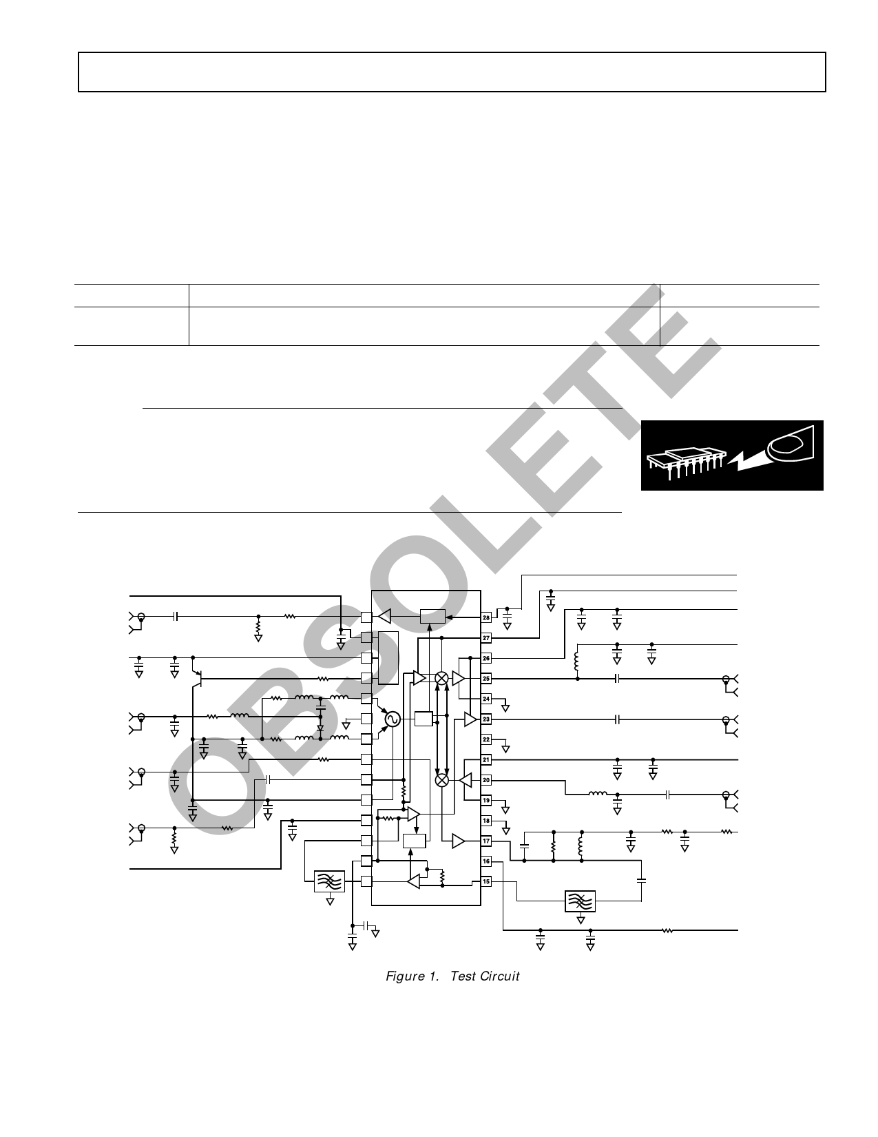
Figure 1. Test Circuit
REV. 0
–3–
Share Link: 