MRFIC0917 Ver la hoja de datos (PDF) - Motorola => Freescale
Número de pieza
componentes Descripción
Fabricante
MRFIC0917
Motorola => Freescale

MRFIC0917 Datasheet PDF : 10 Pages
| |||
MOTOROLA
SEMICONDUCTOR TECHNICAL DATA
Order this document
by MRFIC0917/D
The MRFIC Line
900 MHz GaAs Integrated
Power Amplifier
This integrated circuit is intended for GSM class IV handsets. The device is
specified for 2.5 Watts output power and 43% minimum power added
efficiency under GSM signal conditions at 3.6 Volt supply voltage. To achieve
this superior performance, Motorola’s planar GaAs MESFET process is
employed. The device is packaged in the PFP–16 Power Flat Pack package
which gives excellent thermal performance through a solderable backside
contact.
• Usable Frequency Range 800 to 1000 MHz
• Typical Output Power: 34.5 dBm @ 3.6 Volts
• 43% Minimum Power Added Efficiency
• Low Parasitic, High Thermal Dissipation Package
• Order MRFIC0917R2 for Tape and Reel.
R2 Suffix = 1,500 Units per 16 mm, 13 inch Reel.
• Device Marking = M0917
MRFIC0917
900 MHz
GSM CELLULAR
INTEGRATED POWER AMPLIFIER
GaAs MONOLITHIC
INTEGRATED CIRCUIT
CASE 978–02
(PFP–16)
ABSOLUTE MAXIMUM RATINGS (TA = 25°C unless otherwise noted)
Rating
Supply Voltage, Normal Conditions
Supply Voltage under Load Stress
RF Input Power
Gate Voltage
Ambient Operating Temperature
Storage Temperature
Thermal Resistance, Junction to Case
Symbol
VD1, VD2
VD1, VD2
Pin
VSS
TA
Tstg
RθJC
Value
6
4.5
15
–6
–40 to + 85
– 65 to +150
15
Unit
Vdc
Vdc
dBm
Vdc
°C
°C
°C/W
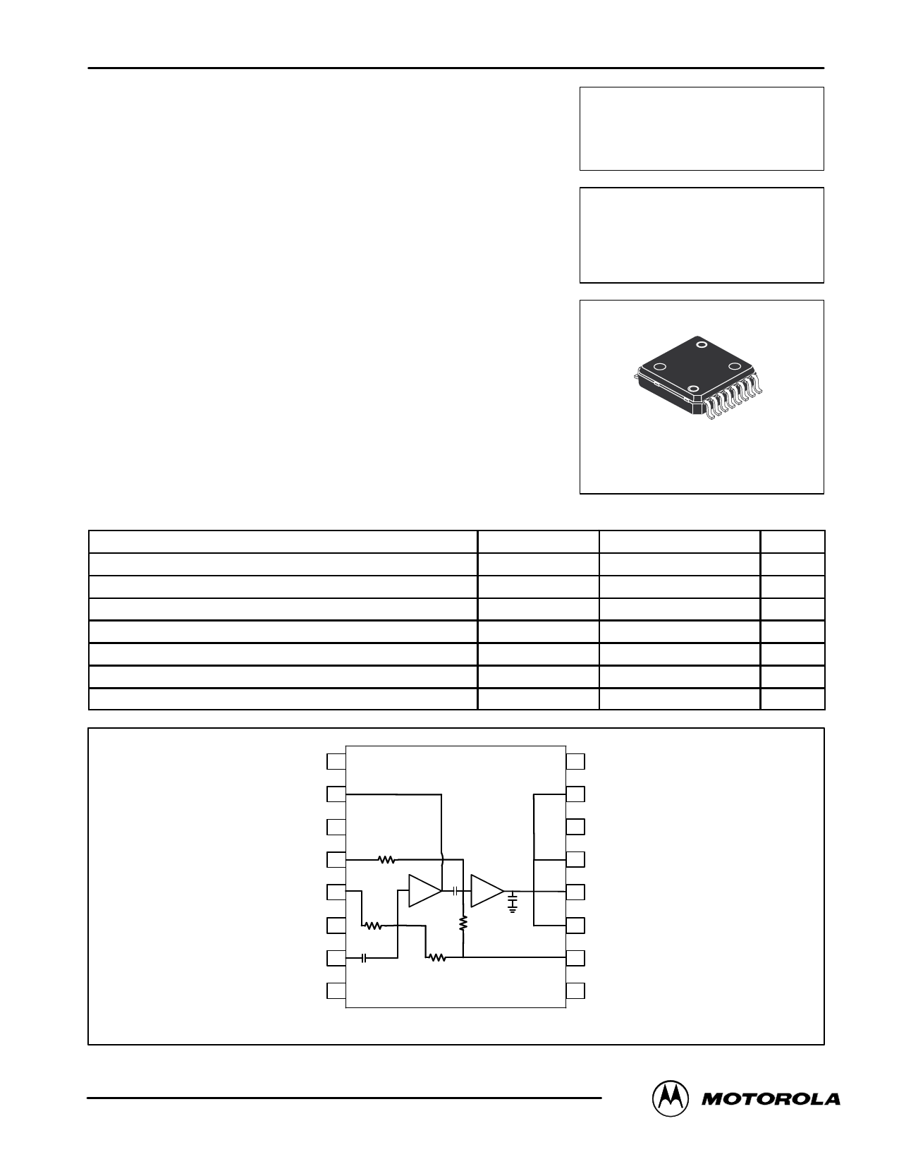
GND 9
VD1 10
GND 11
VG2 12
VG1 13
GND 14
RF IN 15
N/C 16
8 N/C
7 VD2
6 GND
5 RF OUT
4 RF OUT
3 RF OUT
2 VSS
1 GND
Pin Connections and Functional Block Diagram
©MOMoTtoOroRlaO, ILncA. 1R99F8 DEVICE DATA
MRFIC0917
1
Share Link: