SC624 Ver la hoja de datos (PDF) - Semtech Corporation
Número de pieza
componentes Descripción
Fabricante
SC624
Semtech Corporation

SC624 Datasheet PDF : 22 Pages
| |||
SC624
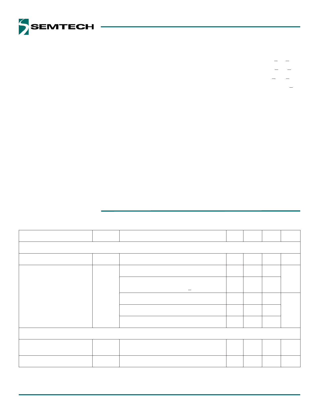
Absolute Maximum Ratings
Recommended Operating Conditions
VIN (V) . . . . . . . . . . . . . . . . . . . . . . . . . . . . . . . . . . . . -0.3 to +6.0
VOUT (V) . . . . . . . . . . . . . . . . . . . . . . . . . . . . . . . . . . -0.3 to +6.0
C1+, C2+ (V) . . . . . . . . . . . . . . . . . . . . . . . -0.3 to (V + 0.3)
OUT
Pin Voltage — All Other Pins (V) . . . . . . . . . -0.3 to (V + 0.3)
IN
VOUT Short Circuit Duration. . . . . . . . . . . . . . . . Continuous
VLDO1, VLDO2 Short Circuit Duration. . . . . . . Continuous
ESD Protection Level(1) (kV) . . . . . . . . . . . . . . . . . . . . . . . . . . . . 2
Ambient Temperature Range (°C) . . . . . . . . -40 < T < +85
A
VIN (V) . . . . . . . . . . . . . . . . . . . . . . . . . . . . . . . . . 3.0 < V < 5.5
IN
VOUT (V) . . . . . . . . . . . . . . . . . . . . . . . . . . . . . . . 2.5 < V < 5.25
OUT
Voltage Difference between any two LEDs (V) . . . . . . <1.2
Thermal Information
Thermal Resistance, Junction to Ambient(2) (°C/W) . . . . 35
Maximum Junction Temperature (°C) . . . . . . . . . . . . . . +150
Storage Temperature Range (°C) . . . . . . . . . . . . -65 to +150
Peak IR Reflow Temperature (10s to 30s) (°C) . . . . . . . +260
Exceeding the above specifications may result in permanent damage to the device or device malfunction. Operation outside of the parameters
specified in the Electrical Characteristics section is not recommended.
NOTES:
(1) Tested according to JEDEC standard JESD22-A114-B.
(2) Calculated from package in still air, mounted to 3” x 4.5”, 4 layer FR4 PCB with thermal vias under the exposed pad per JESD51 standards.
Electrical Characteristics
Unless otherwise noted, T = +25°C for Typ, -40ºC to +85°C for Min and Max, T = 125ºC, V = 3.0V to 4.2V, C = C = C = 2.2μF,
A
J(MAX)
IN
IN
1
2
C = 4.7μF (ESR = 0.03Ω), ΔV ≤ 1.2V(1)
OUT
F
Parameter
Symbol
Conditions
Min Typ Max Units
Supply Specifications
Shutdown Current
Total Quiescent Current
I
Q(OFF)
I
Q
Shutdown, V = 4.2V
IN
Sleep (LDOs off ), SWIF = V
IN
Sleep (LDOs on), SWIF = V ,
IN
V > (V + 300mV), I < 200mA
IN
LDO
LDO
Charge pump in 1x mode, 4 backlights on
0.1
2
μA
100 160
μA
220 340
3.8 4.65
Charge pump in 1.5x mode, 4 backlights on
4.6 5.85 mA
Charge pump in 2x mode, 4 backlights on
4.6 5.85
Fault Protection
Output Short Circuit
Current Limit
Over-Temperature
I
OUT(SC)
T
OTP
VOUT pin shorted to GND
300
mA
160
°C
3
Share Link: