SC1456 Ver la hoja de datos (PDF) - Semtech Corporation
Número de pieza
componentes Descripción
Fabricante
SC1456 Datasheet PDF : 10 Pages
| |||
POWER MANAGEMENT
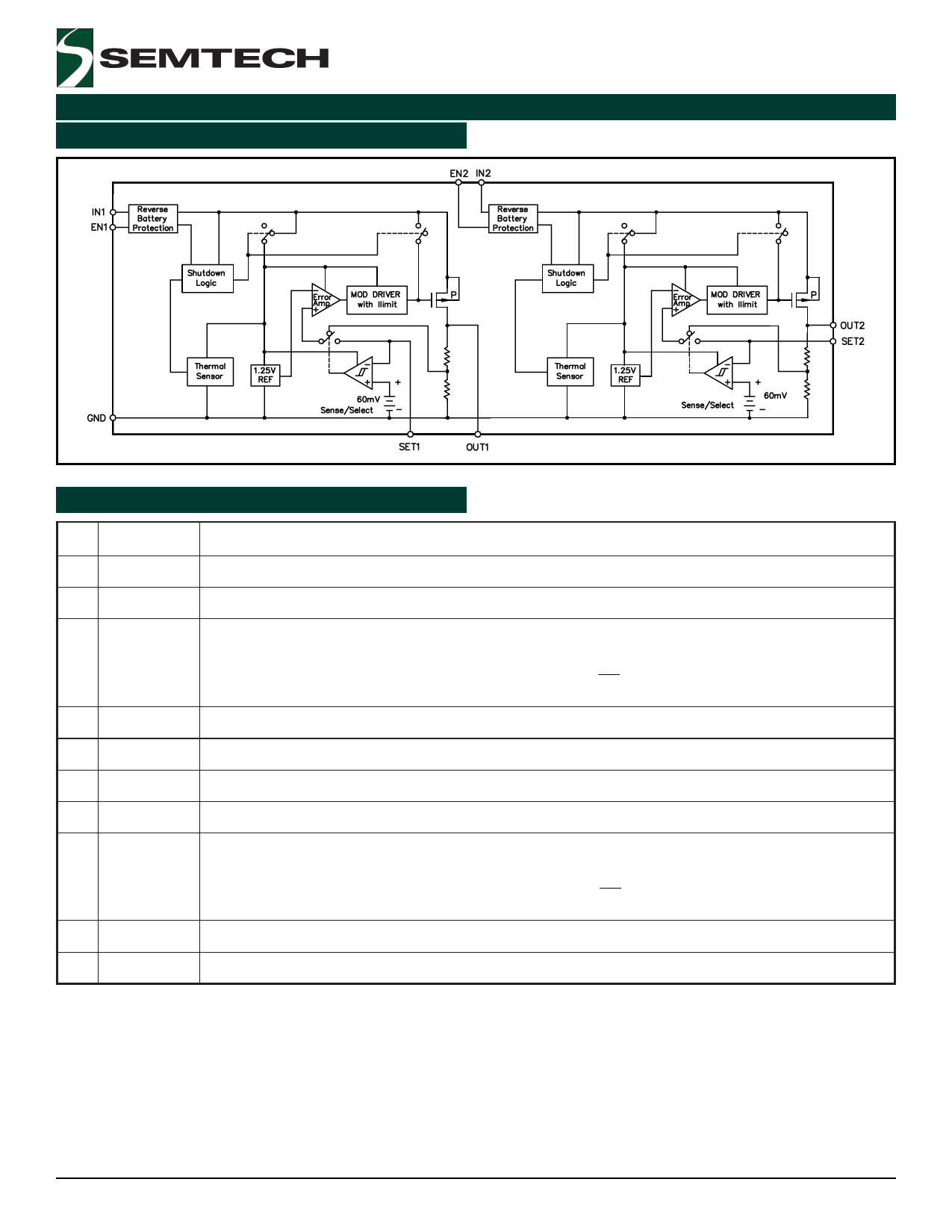
Block Diagram
SC1456
Pin Descriptions
Pin Pin Name Pin Function
1
EN1
Active high enable pin for device 1. Connect to VIN1 if not being used.
2
GND
Ground pin. Can be used for heatsinking if needed. Electrically connected to pin 7.
3
SET 1 Connecting this pin to ground results in the internally preset value for VOUT1. Connecting to an external
resistor divider changes VOUT1 to:
VOUT 1
=
1.250
•
1 +
R1
R2
4
OUT2 Regulator output for device 2, sourcing up to 150mA.
5
IN2
Supply input pin for device 2.
6
EN2
Active high enable pin for device 2. Connect to VIN2 if not being used.
7
GND
Ground pin. Can be used for heatsinking if needed. Electrically connected to pin 2.
8
SET2
Connecting this pin to ground results in the internally preset value for VOUT2. Connecting to an external
resistor divider changes VOUT2 to:
VOUT 2
=
1.250
• 1 +
R1
R2
9
OUT1 Regulator output for device 1, sourcing up to 150mA
10
IN1
Supply input pin for device 1.
2005 Semtech Corp.
5
www.semtech.com
Share Link: 