SAA1305T Ver la hoja de datos (PDF) - Panasonic Corporation
Número de pieza
componentes Descripción
Fabricante
SAA1305T Datasheet PDF : 32 Pages
| |||
Philips Semiconductors
On/off logic IC
Product specification
SAA1305T
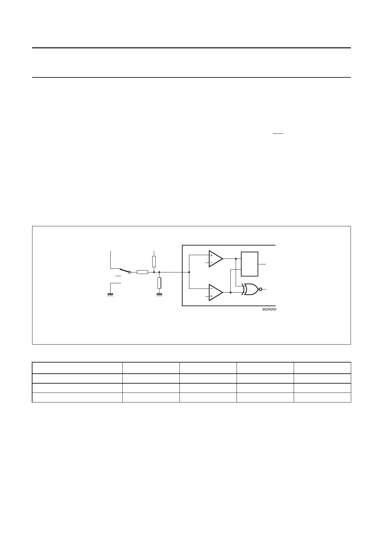
IMPEDANCE DETECTION
Input D1 is a normal input with comparable behaviour like
the other seven inputs. The only difference is an additional
internal exclusive-NOR (EXNOR) connected between the
two comparator outputs for high and low detection;
see Fig.4. The EXNOR signal indicates, in combination
with a special external circuit on input D1, a voltage of
1⁄2VDD on this input.
The simple input description for impedance detection is
probably not the real solution, but helps to explain the
function. Input D1 can be used as a normal input and for
impedance detection as described in Table 2. For normal
use the output Q acts like every other input, but for
impedance detection the EXNOR output S is also
important. Output S is linked to the status register bit 6 and
indicates the 1⁄2VDD; see Table 5.
Between detection and indication via the status register
bit 6, a delay time is integrated (programmable via the
impedance register bits 1 and 0; see Table 15). When the
1⁄2VDD value is detected the EXNOR output will be set to
logic 1 (active) and after the programmed delay time the
status register bit 6 will be set to logic 1 (active). This event
will also be indicated via pin CHI and (if enabled) pin RP.
The impedance information (bit 6 is active) within the
status register is present until the I2C-bus status is read.
With the disappearance of the impedance information no
further actions will be generated. Every impedance signal
change during the delay time will restart the delay time.
However an impedance detection is only possible in the
event of a stable signal, at least for the programmed delay
time. Setting the status register bit 6 with a repetition time
which equals the ‘impedance delay time’ as long as
input D1 stays in high-impedance state is implemented.
handbook, full pagewidth
12 V
5V
ignition
key 10 kΩ
100 kΩ
input D1
100 kΩ
3.5 V
1.5 V
O1
S
Q
R
O2
S
MGR203
Fig.4 Simple input description for impedance detection.
Table 2 Logic levels for impedance detection
IGNITION KEY
O1
O2
Q
S
12 V
1
0
1
0
Open-circuit (VI = 2.5 V)
0
Ground (VI < 1.5 V)
0
0
0 or 1
1
1
0
0
2004 Jan 15
8
Share Link: 