SA9604 Ver la hoja de datos (PDF) - South African Micro Electronic Systems
Número de pieza
componentes Descripción
Fabricante
SA9604
South African Micro Electronic Systems

SA9604 Datasheet PDF : 20 Pages
| |||
SA9604A
Address locations A4 and A5 have been included to ensure compatibility with future
SAMES integrated circuit developments.
When CS is high, data input on pin DI is clocked into the device on the rising edge
of SCK. The data clocked into DI will comprise of 1 1 0 A5 A4 A3 A2 A1 A0, in this
order.
5.3 Data Output
After the least significant digit of the address has been entered on the rising edge
of SCK, the output DO goes low with falling edge of SCK. Each subsequent falling
edge transaction on the SCK pin will validate data of the register contents on pin DO.
The contents of each register consists of 24 bits of data output on pin D0, starting
with the most significant digit, D23.
5.4 Frequency Register
For the frequency register only bits D15 ... D0 are used for calculations. The upper
seven bits (D23 ... D17) must still be clocked out, as important frequency information
can be derived from these data bits.
Bit D17 changes with every rising edge of the mains voltage (25Hz square wave for
50Hz mains system). Bit D18 displays a frequency of D17/2 and D19 displays a
frequency of D17/4.
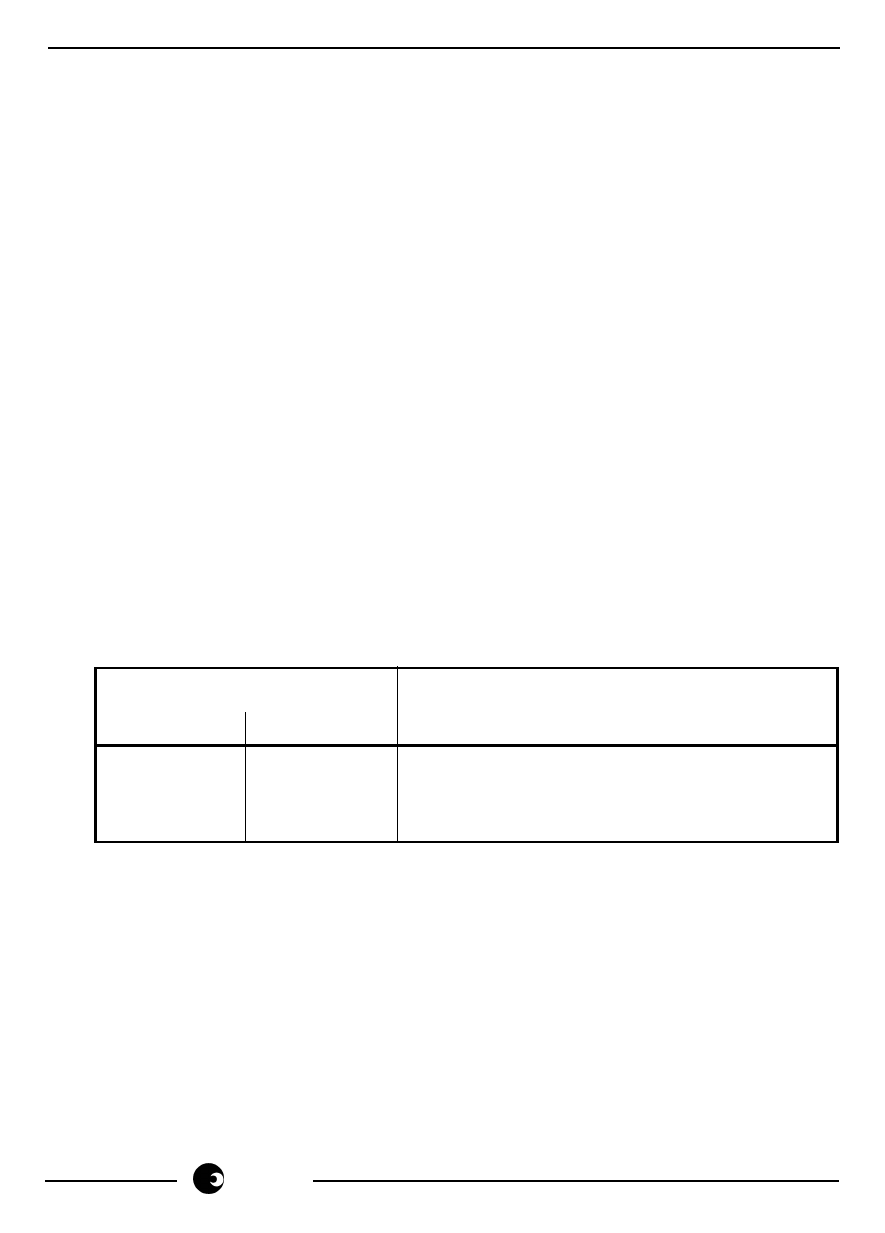
The phase error status may be ascertained from bits D20 and D21. The table below
may be used for this purpose:
Frequency data Bits
D21
D20
Description
0
0
No phase error
1
0
Phase sequence error (2 phase swapped)
1
1
Missing phase
The phase error status is merged on all three frequency registers.
Bits D16, D22 and D23 are not used.
sames
7/20
Share Link: