SA8281/IG/DP1S Ver la hoja de datos (PDF) - Mitel Networks
Número de pieza
componentes Descripción
Fabricante
SA8281/IG/DP1S Datasheet PDF : 14 Pages
| |||
SA828
HARDWARE INPUT/OUTPUT FUNCTIONS
Set Output Trip (SET TRIP input)
The SET TRIP input is provided separately from the
microprocessor interface in order to allow an external source
to override the microprocessor and provide a rapid shutdown
facility. For example, logic signals from overcurrent sensing
circuitry or the microprocessor ‘watchdog’ might be used to
activate this input.
When the SET TRIP input is taken to a logic high, the output
trip latch is activated. This results in the TRIP output and the
six PWM outputs being latched low immediately. This condition
can only be cleared by applying a reset cycle to the RST input.
It is essential that when not in use SET TRIP is tied low and
isolated from potential sources of noise; on no account should
it be left floating.
SET TRIP is latched internally at the master clock rate in
order to reduce noise sensitivity.
Output Trip Status (TRIP output)
The TRIP output indicates the status of the output trip latch
and is active low.
Reset (RST input)
The RST input performs the following functions when active
(low):
1. All PWM outputs are forced low (if not already low) thereby
turning off the drive switches.
2. All internal counters are reset to zero (this corresponds to 0°
for the red phase output).
3. The rising edge of RST reactivates the PWM outputs
resetting the output trip and setting the TRIP output high –
assuming that the SET TRIP input is inactive (i.e. Iow).
A sixth register, R5, located at A2:O = 101 is used to place
the device into a factory test mode. This is achieved by writing
dummy data to R5 immediately after RST goes high. Care
must be exercised to ensure that the microprocessor/controller
cannot write to this register.
Zero Phase Pulses (ZPPR, ZPPY and ZPPB outputs)
The zero phase pulse outputs provide pulses at the same
frequency as the power frequency with a 1 : 2 mark-space
ratio. When in the forward mode of operation the falling edge
of ZPPR corresponds to 0° for the red phase, the falling edge
of ZPPY to 0° for the yellow phase and the ZPPB falling edge
to 0° for the blue phase. In the reverse mode, the rising edge
of a zero phase pulse corresponds to 0° for the relevant phase
PWM output.
Waveform Sampling Synchronisation (WSS output)
This output provides a square wave signal of 50% duty
cycle at a frequency 1536 times higher than the fundamental
of the power waveform. Each successive pulse of WSS
corresponds to the SA828 reading the next location of the
waveform ROM. It may be used in conjunction with the ZPP
signals to monitor the position of the machine rotor and may
form part of a closed loop control system such as slip
compensation.
Clock (CLK input)
The CLK input provides a timing reference used by the
SA828 for all timings related to the PWM outputs. The
microprocessor interface, however, derives all its timings from
the microprocessor and therefore the microprocessor and the
SA828 may be run either from the same or from different
clocks.
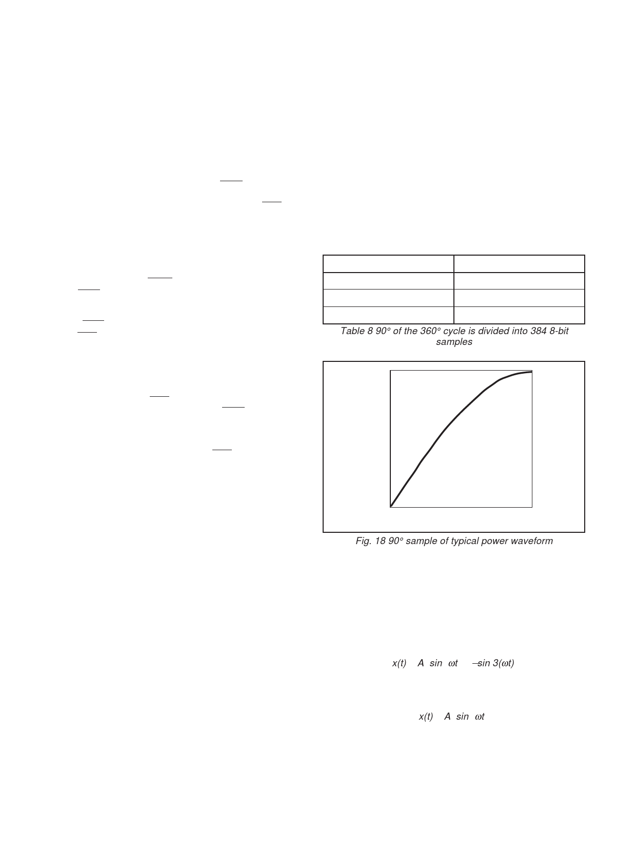
WAVEFORM DEFINITION
The waveform amplitude data used to construct the PWM
output sequences is read from the internal 384X8 ROM. This
contains the 90° span of the waveform as shown in Fig. 18.
Each successive 8-bit sample linearly represents the
instantaneous amplitude of the waveform. It is assumed that
the waveform is symmetrical about the 90°, 180° and 270° axes.
The SA828 reconstructs the full 360° waveform by reading the
0°-90° section held in ROM and assigning negative values for
the second half of the cycle.
These samples are used to calculate the instantaneous
amplitudes for all three phases, which will be 120° transposed
in the normal R-Y-B orientation for forward rotation or B-Y-R for
reverse rotation. The 384 8-bit samples are regularly spaced
over the 0° to 90° span, giving an angular resolution of
approximately 0·23°.
Waveform segment
Sample number
0°- 30°
0 - 127
30·23°- 60°
128 - 255
60·23°- 89·77°
256 - 383
Table 8 90° of the 360° cycle is divided into 384 8-bit
samples
255
VALUE
OF
8-BIT
SAMPLE
POWER
WAVEFORM
0
0°
45°
90°
PHASE (384-BIT RESOLUTION)
Fig. 18 90° sample of typical power waveform
PRODUCT DESIGNATION
Two standard options exist, defining waveform shape. These
are designated SA828-1 and SA828-2 as follows:
SA828-1
Sine + third harmonic at one-sixth the amplitude of the
fundamental:
x(t) = A [sin (ωt) + 16sin 3(ωt)]
SA828-2
Pure sinewave:
x(t) = A [sin (ωt)]
Additional wave shapes can be implemented to order, provided
they are symmetrical about the 90°, 180° and 270° axes.
Contact your local Mitel Semiconductor Customer Service
Centre for further details.
10
Share Link: 