S2100 Ver la hoja de datos (PDF) - Seiko Instruments Inc
Número de pieza
componentes Descripción
Fabricante
S2100 Datasheet PDF : 9 Pages
| |||
64-bit FUSE ROM
S-2100R
n Program Mode Operation
By setting the CE/PE terminal to “H” level, the S-2100R enters the counter hold mode and at the same time enters the program
mode. *5
Writing is done in program mode after selecting the address in read mode. *6 Select the address, and supply “H” level to the
CE/PE terminal and “L” level to the DATA terminal, with the writing pulse VPP being supplied to the PD/VPP terminal. “L” level can
be written into the selected address only once. *7 *8
If you coutinue writing from address 1 to 64, the output of the COUNTER OUT terminal goes to “H” level, just like in the read mode,
and no more CLK pulses or writing pulses in program mode can be accepted.
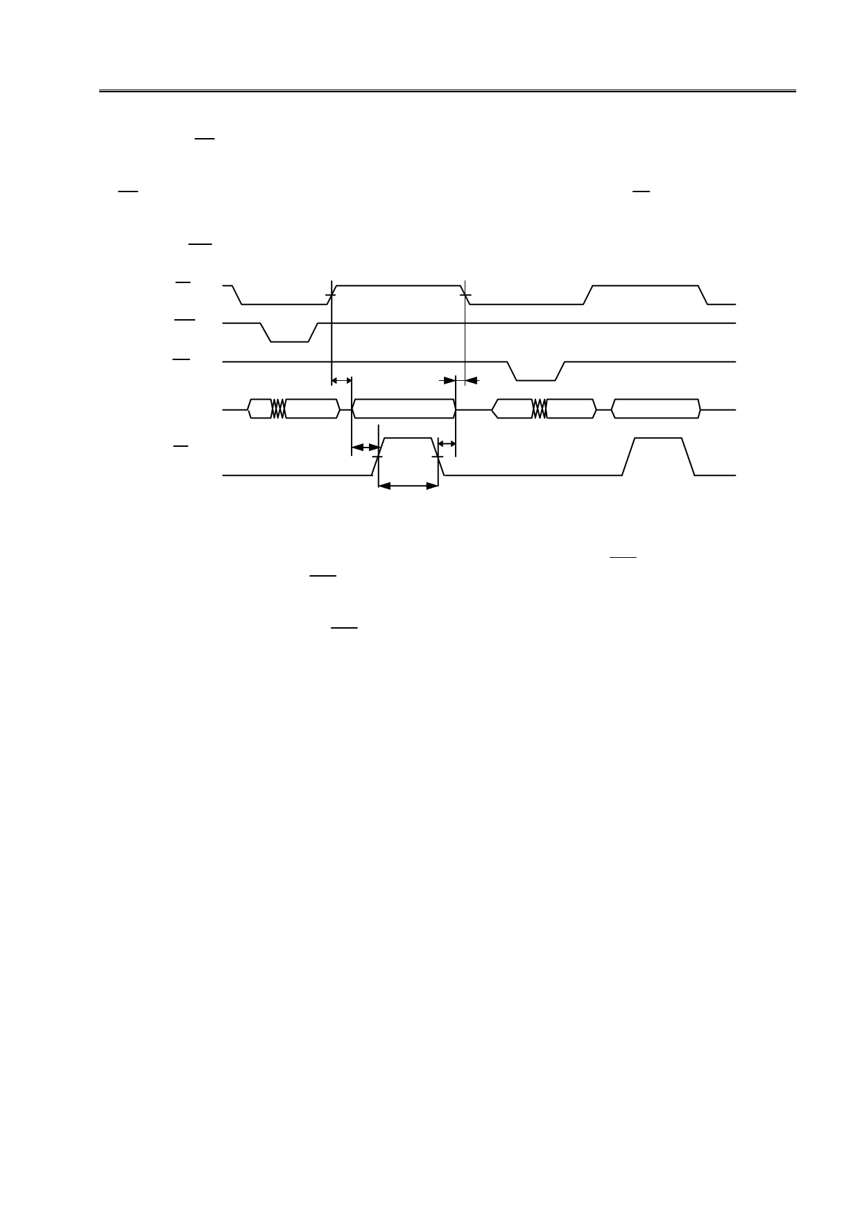
CE/P
RS
CL
DATA
PD/VPP
tCDS
tCDH
Address 1
output
Data input
tDS
tDH
Address 1
output
Address 2
output
tPW
Figure 5 Program mode timing
Data input
*5 In program mode, operate at VDD=5.0 V to assure reliability of the data writing.
*6 The selection of addresses is possible only in read mode. Address 1 is selected by RST pulses and writing proceeds
sequentially from address 1 by CLK pulse.
*7 All the memories are initially at “H” level, so writing into “L” can be done. When data is at “H” level, writing voltage cannot
be supplied to the memory.
*8 Address 1 is selected again by the RST pulse. The addresses which are not written to “L” level are at “H” level, so writing
“L” level in these addresses is possible.
Seiko Instruments Inc.
5
Share Link: 