RT9204A Ver la hoja de datos (PDF) - Richtek Technology
Número de pieza
componentes Descripción
Fabricante
RT9204A Datasheet PDF : 14 Pages
| |||
Preliminary
RT9204/A
Input / Output Capacitor
High frequency/long life decoupling capacitors should be
placed as close to the power pins of the load as physically
possible. Be careful not to add inductance to the PCB
trace, as it could eliminate the performance from utilizing
these low inductance components. Consult with the
manuf acturer of the load on specific decoupling
requirements.
The output capacitors are necessary for filtering output
and stabilizing the close loop (see the PWM loop stability).
For powering advanced, high-speed processors, it is
required to meet with the requirement of fast load transient,
high frequency capacitors with low ESR/ESL capacitors
are recommended.
Another concern is high ESR induced ripple may trigger
UV or OV protections.
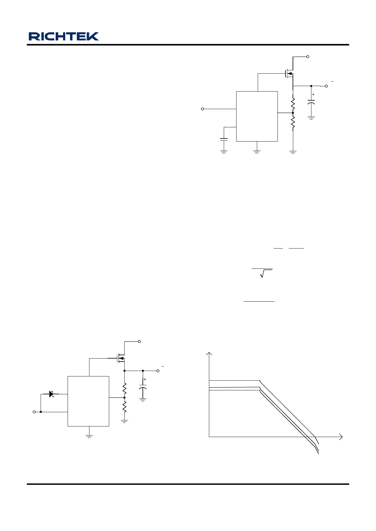
Linear Regulator Driver
The linear regulator of RT9204/A was designed to drive
bipolar NPN or MOSFET pass transistor. For MOSFET
pass transistor, normally DRV need to provide minimum
VOUT2+VT+gate-drive voltage to keep VOUT2 as setting
voltage. When driving MOSFET operating at 5V power
supply system, the gate-drive will be limited at 5V. In this
situation shown in Figure 5, low VT threshold MOSFET
(VT = 1V) and Vout2 setting below 2.5V were suggested.
In VBOOT = 12V operation condition as Figure 8, VCC is
regulated as higher to 6V providing more gate-drive for
pass MOSFET transistor, VOUT2 can be set as ≤ 3.3V.
VOUT2 < 3.3V
VBOOT = 12V
DRV
BOOT
FBL
6V VCC
RT9204/A
R3
R4
R4<1K
Figure 8
PWM Loop Stability
The RT9204/A is a voltage mode buck controller designed
for 5V step-down applications. The gain of error amplifier
is fixed at 35dB for simplified design.
The output amplitude of ramp oscillator is 1.6V, the loop
gain and loop pole/zero are calculated as follows:
5 0.8
DC loop gain GA = 35 dB × ×
1.6 VOUT
1
LC filter pole PO =
2π LC
Error Amp pole PA = 300kHz
1
ESR zero ZO =
2πESR × C
The RT9204/A Bode plot as shown Figure 9. is stable in
most of application conditions.
VCC = 5V
VOUT2 < 2.5V
DRV
BOOT
FBL
VCC
RT9204/A
R3
R4 R4<1K
Figure 7
VOUT = 3.3V
COUT = 1500uF(33mΩ)
L = 2uH
40
VOUT = 1.5V
VOUT = 2.5V
30 VOUT = 3.3V
PO = 2.9kHz
ZO = 3.2kHz
20
Loop Gain
10
100
1k
10k
100k
1M
Figure 9
DS9204/A-08 March 2007
www.richtek.com
11
Share Link: 