RT9201 Ver la hoja de datos (PDF) - Richtek Technology
Número de pieza
componentes Descripción
Fabricante
RT9201 Datasheet PDF : 13 Pages
| |||
RT9201
Absolute Maximum Ratings (Note 1)
l Input Voltage ---------------------------------------------------------------------------------------------------------- 6V
l Power Dissipation, PD @ TA = 25°C
VDFN−10L 3x3 ------------------------------------------------------------------------------------------------------- 2.1W
l Junction Temperature ----------------------------------------------------------------------------------------------- 150°C
l Storage Temperature Range --------------------------------------------------------------------------------------- −65°C to 150°C
l Package Thermal Resistance
VDFN−10L 3x3, θJA -------------------------------------------------------------------------------------------------- 47°C/W
l Lead Temperature (Soldering, 10 sec.) -------------------------------------------------------------------------- 260°C
l Storage Temperature Range --------------------------------------------------------------------------------------- −65°C to 150°C
l ESD Susceptibility (Note 2)
HBM (Human Body Mod) ----------------------------------------------------------------------------------------- 2kV
MM (Machine Mode) ----------------------------------------------------------------------------------------------- 200V
Recommended Operating Conditions (Note 3)
l Supply Input Voltage ------------------------------------------------------------------------------------------------ 2.5V to 5.5V
l Junction Temperature Range -------------------------------------------------------------------------------------- −40°C to 125°C
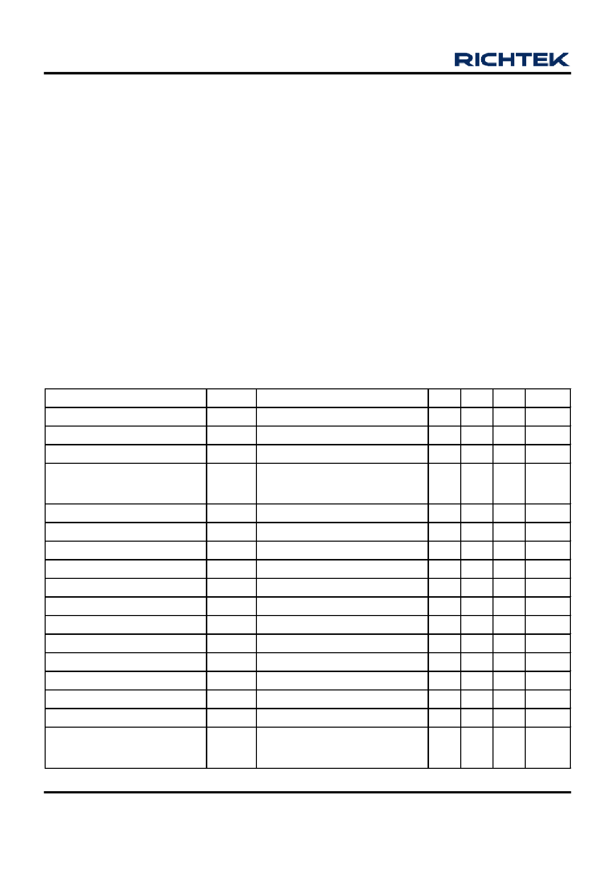
Electrical Characteristics
(VIN = 3.6V, VOUT = 2.5V, EN = VIN, LX = 10µH, CIN = 10µF, COUT = 22µF, TA = 25° C, unless otherwise specified)
Parameter
Symbol
Test Conditions
Min Typ Max
Input Voltage Range
Adjustable Output Range
Reference Voltage
VIN
VOUT
VREF
(Note 4)
IL = 300mA
2.5 -- 5.5
0.85 -- VIN
-- 0.8 --
Cross Regulation
∆VCROSS
VIN = 2.5V to 5.5V,
IL = 600mA to 0mA
−3 -- +3
Units
V
V
V
%
FB Input Current
PMOSFET RON
NMOSFET RON
P-Channel Current Limit
Quiescent Current
Shutdown Current
Oscillator Frequency
EN Input High Threshold
EN Input Low Threshold
Thermal Shutdown Temperature
Maximum Duty Cycle
Minimum On Time
IFB
VFB = VIN
PRDS(ON) ILX = 200mA
NRDS(ON) ILX = 200mA
IP(LM)
RL = 0.1 Ω, VFB = VREF − 0.15
IQ
ILX = 0mA, VFB = VREF + 0.15
IQ(SD) EN = 0V, VIN = 5.5V
fOSC
IOUT = 100mA
VIH
VIN = 2.5V to 5.5V
VIL
VIN = 2.5V to 5.5V
TSD
VIN = VOUT
No Load
LX Leakage Current
EN = 0V,VIN = 5.5V, VLX = 0V or
VLX = 5.5V
−50 -- 50
nA
0.2 0.37 0.43 Ω
0.2 0.3 0.35 Ω
0.8 1.17 1.6
A
40 85 140 µA
0.01 2
7
µA
600 800 1k kHz
1.5 -- --
V
-- -- 0.4
V
125 150 --
°C
100 -- --
%
0.1 0.2 0.3
µs
−20 1 20
µA
www.richtek.com
4
DS9201-12 August 2007
Share Link: 