RT9183 Ver la hoja de datos (PDF) - Richtek Technology
Número de pieza
componentes Descripción
Fabricante
RT9183 Datasheet PDF : 17 Pages
| |||
VIN
Enable
C
0.1uF
(SOP-8 & TO-263-5)
RT9183
VIN
VOUT
CIN EN
10uF
GND ADJ
VOUT
COUT
10uF
Figure 3. Fixed Operation with SOP-8 and TO-263-5 packages
Functional Pin Description
Pin Name
Pin Function
Chip Enable Control Input.
EN
Note that the device will be in the unstable state if the pin is not connected.
VIN
Supply Input.
GND
Common Ground.
VOUT
ADJ
Regulator Output.
The output voltage is set by the internal feedback resistors when this pin
grounded. If external feedback resistors are applied, the output voltage will be:
VOUT = 0.8 × (1 + R1) Volts
R2
RT9183
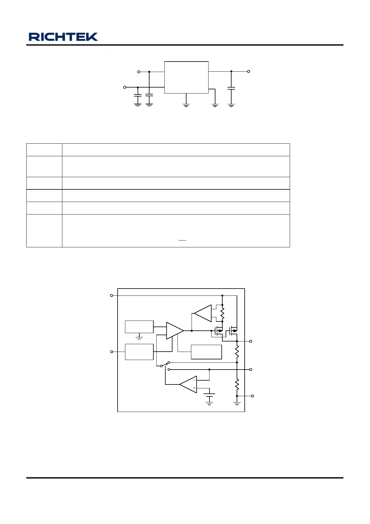
Function Block Diagram
VIN
Current Limit
Sensor
+
Error
Amplifier
-
0.8V
Reference
-
+
EN
Shutdown
Logic
Thermal
Shutdown
Output Mode
Comparator
100mV
VOUT
ADJ
GND
DS9183-14 April 2008
www.richtek.com
3
Share Link: 