RT8251GSP Ver la hoja de datos (PDF) - Richtek Technology
Número de pieza
componentes Descripción
Fabricante
RT8251GSP Datasheet PDF : 16 Pages
| |||
RT8251
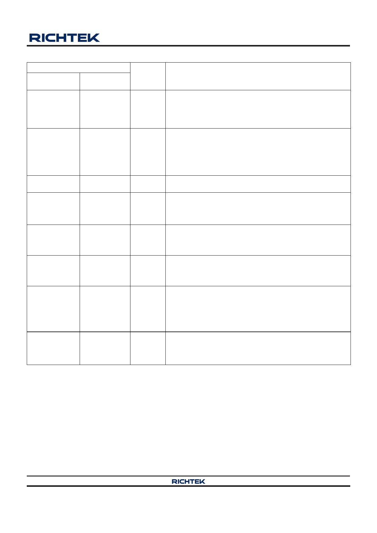
Functional Pin Description
Pin No.
WQFN-16L 3x3
SOP-8
Pin Name
(Exposed Pad)
1, 2, 3, 15, 16
2
VIN
4,
17 (Exposed Pad)
9
4,
(Exposed
Pad)
GND
Pin Function
Power Input. VIN supplies the power to the IC, as well as the
step-down converter switches. Connect VIN with a 4.75V to 24V
power source. Connect VIN to GND with a capacitor that the
capacitance is large enough to eliminate noise on the input to the
IC.
Ground. This pin is the voltage reference for the regulated output
voltage. For this reason, care must be taken in its layout. This
node should be placed outside of the D1 to CIN ground path to
prevent switching current spikes from inducing voltage noise into
the part. The exposed pad must be soldered to a large PCB and
connected to GND for maximum power dissipation.
5
5
FB
Feedback Input. An external resistor divider from the output to
GND, tapped to the FB pin, sets the output voltage.
Compensation Node. This node is the output of the
6
6
COMP
transconductance error amplifier and the input to the current
comparator. Frequency compensation is done at this node by
connecting a series R-C to ground.
Enable Input. EN is a digital input that turns the regulator on or
7
7
EN
off. Drive EN higher than 1.4V to turn on the regulator, lower
than 0.4V to turn it off. For automatic startup, leave EN
unconnected.
Soft-Start Control Input. SS controls the soft start period.
8
8
SS
Connect a capacitor (≧10nF) from SS to GND to set the
soft-start period. A 10nF capacitor sets the Soft-Start period to
1ms.
Bootstrap. This capacitor CBOOT is needed to drive the power
switch’s gate above the supply voltage. It is connected between
9
1
BOOT
the SW and BS pins to form a floating supply across the power
switch driver. The voltage across CBOOT is about 5V and is
supplied by the internal +5V supply when the SW pin voltage is
low.
10, 11, 12, 13,
14
Power Switching Output. SW is the switching node that supplies
3
SW
power to the output. Connect the output LC filter from SW to the
output load. Note that a capacitor is required from SW to BOOT
to power the high-side switch.
Copyright ©2013 Richtek Technology Corporation. All rights reserved.
DS8251-04 February 2013
is a registered trademark of Richtek Technology Corporation.
www.richtek.com
3
Share Link: 