RT8250GSP Ver la hoja de datos (PDF) - Richtek Technology
Número de pieza
componentes Descripción
Fabricante
RT8250GSP Datasheet PDF : 12 Pages
| |||
RT8250
Thermal Considerations
For continuous operation, do not exceed the maximum
operation junction temperature 125°C. The maximum
power dissipation depends on the thermal resistance of
IC package, PCB layout, the rate of surroundings airflow
and temperature difference between junction to ambient.
The maximum power dissipation can be calculated by
following formula :
PD(MAX) = ( TJ(MAX) − TA ) / θJA
Where TJ(MAX) is the maximum operation junction
temperature, TA is the ambient temperature and the θJA is
the junction to ambient thermal resistance.
For recommended operating conditions specification of
RT8250, the maximum junction temperature is 125°C. The
junction to ambient thermal resistance θJA is layout
dependent. For PSOP-8 package, the thermal resistance
θJA is 75°C/W on the standard JEDEC 51-7 four-layers
thermal test board. The maximum power dissipation at TA
= 25°C can be calculated by following formula :
PD(MAX) = (125°C − 25°C) / (75°C/W) = 1.333W for
PSOP-8 package
The maximum power dissipation depends on operating
ambient temperature for fixed TJ(MAX) and thermal
resistance θJA. For RT8250 package, the Figure 3 of
derating curve allows the designer to see the effect of
rising ambient temperature on the maximum power
dissipation allowed.
1.6
1.4
1.2
1.0
0.8
0.6
0.4
0.2
0.0
0
Four-Layer PCB
25
50
75
100
125
Ambient Temperature (°C)
Figure 3. Derating Curve for RT8250 Package
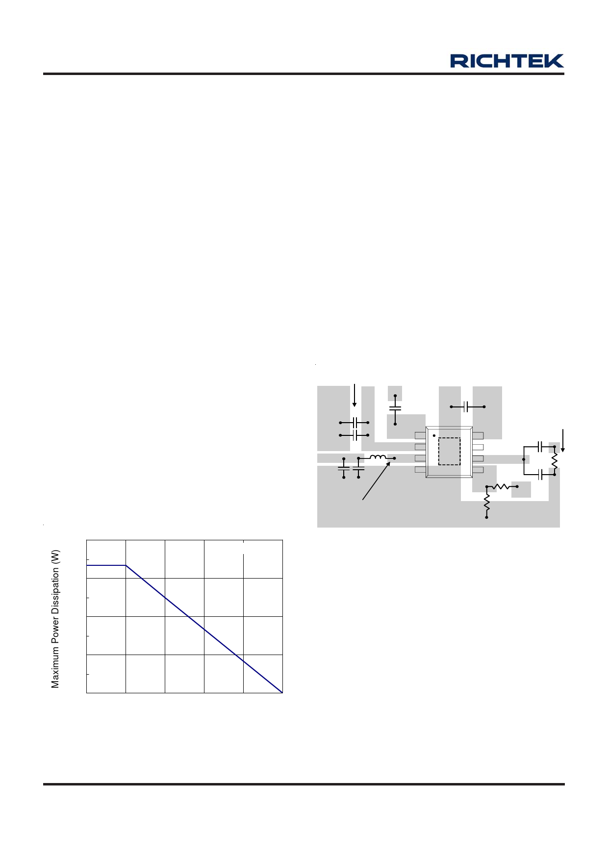
Layout Consideration
Follow the PCB layout guidelines for optimal performance
of the RT8250.
` Keep the traces of the main current paths as short and
wide as possible.
` Put the input capacitor as close as possible to the device
pins (VIN and GND).
` SW node is with high frequency voltage swing and
should be kept at small area. Keep sensitive
components away from the SW node to prevent stray
capacitive noise pick-up.
` Place the feedback components to the FB pin and
COMP pin as close as possible.
` The GND pin and Exposed Pad should be connected to
a strong ground plane for heat sinking and noise
protection.
Input capacitor must be placed
as close to the IC as possible.
GND
VIN SW
CS
CIN
VOUT
COUT
BOOT
L1
VIN
SW
GND
8
2 GND 7
3
6
4
5
The feedback
components must be
connected as close to
the device as possible.
SS
CC
EN
COMP
FB
CP RC
R1
SW should be connected to inductor by
R2
wide and short trace. Keep sensitive
components away from this trace.
VOUT
GND
Figure 4. PCB Layout Guide
www.richtek.com
10
DS8250-05 March 2011
Share Link: 