RT8294GSP Ver la hoja de datos (PDF) - Richtek Technology
Número de pieza
componentes Descripción
Fabricante
RT8294GSP Datasheet PDF : 15 Pages
| |||
RT8294
Absolute Maximum Ratings (Note 1)
l Supply Voltage, VIN ---------------------------------------------------------------------------------------------- −0.3V to 25V
l Input Voltage, SW ------------------------------------------------------------------------------------------------ −0.3V to (VIN + 0.3V)
l VBOOT − VSW ------------------------------------------------------------------------------------------------------- −0.3V to 6V
l Other Pins Voltages ---------------------------------------------------------------------------------------------- −0.3V to 6V
l Power Dissipation, PD @ TA = 25°C
SOP-8 ---------------------------------------------------------------------------------------------------------------- 1.111W
SOP-8 (Exposed Pad) -------------------------------------------------------------------------------------------- 1.333W
l Package Thermal Resistance (Note 2)
SOP-8, θJA ---------------------------------------------------------------------------------------------------------- 90°C/W
SOP-8 (Exposed Pad), θJA -------------------------------------------------------------------------------------- 75°C
SOP-8 (Exposed Pad), θJC -------------------------------------------------------------------------------------- 15°C
l Junction Temperature -------------------------------------------------------------------------------------------- 150°C
l Lead Temperature (Soldering, 10 sec.) ----------------------------------------------------------------------- 260°C
l Storage Temperature Range ------------------------------------------------------------------------------------ −65°C to 150°C
l ESD Susceptibility (Note 3)
HBM (Human Body Mode) -------------------------------------------------------------------------------------- 2kV
MM (Machine Mode) --------------------------------------------------------------------------------------------- 200V
Recommended Operating Conditions (Note 4)
l Supply Voltage, VIN ---------------------------------------------------------------------------------------------- 4.5V to 23V
l Junction Temperature Range ----------------------------------------------------------------------------------- −40°C to 125°C
l Ambient Temperature Range ----------------------------------------------------------------------------------- −40°C to 85°C
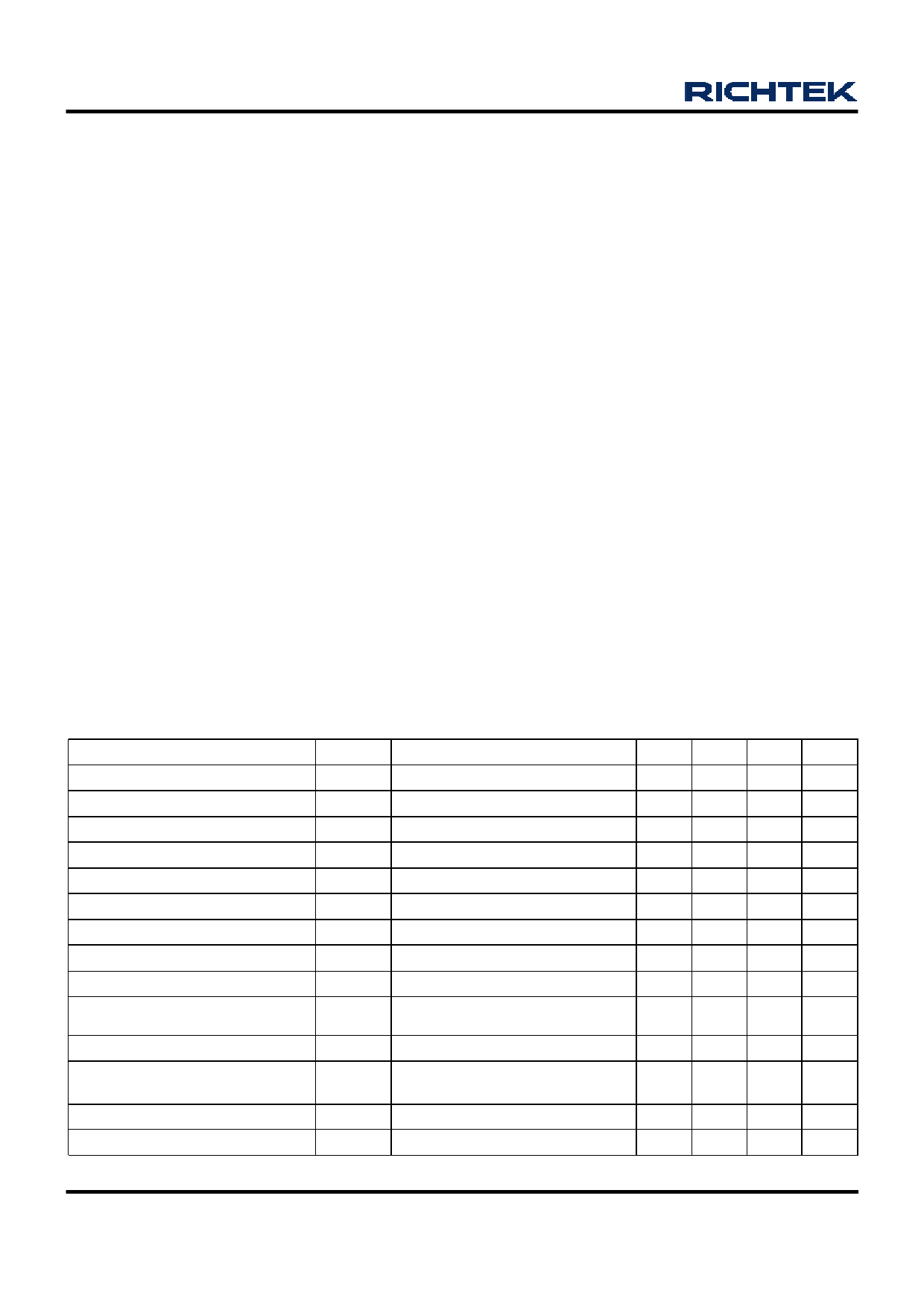
Electrical Characteristics
(VIN = 12V, TA = 25°C unless otherwise specified)
Parameter
Symbol
Test Conditions
Min
Shutdown Supply Current
VEN = 0V
--
Supply Current
ICC
Feedback Voltage
VFB
Error Amplifier Transconductance GEA
VEN = 3 V, VFB = 1V
4.5V ≦ VIN ≦ 23V
ΔIC = ± 10µA
--
0.909
--
High-Side Switch-On Resistance RDS(ON)1
--
Low-Side Switch-On Resistance RDS(ON)2
--
High-Side Switch Leakage Current
VEN = 0V, VSW = 0V
--
Upper Switch Current Limit
Low Switch Current Limit
Min.Duty Cycle, VBOOT−SW = 4.8V --
From Drain to Source
--
COMP to Current Sense
Transconductance
GCS
--
Oscillator Frequency
fOSC1
300
Short Circuit Oscillation
Frequency
fOSC2
VFB = 0V
--
Maximum Duty Cycle
DMAX
VFB = 0.7V
--
Minimum On-Time
tON
--
Typ Max
0.5
3
0.8 1.2
0.923 0.937
940 --
130 --
130 --
0
10
4.3
--
1.3
--
4
--
340 380
100 --
93
--
100 --
Unit
µA
mA
V
µA/V
mΩ
mΩ
µA
A
A
A/V
kHz
kHz
%
ns
www.richtek.com
4
To be continued
DS8294-02 March 2011
Share Link: 