RT8269GSP Ver la hoja de datos (PDF) - Richtek Technology
Número de pieza
componentes Descripción
Fabricante
RT8269GSP Datasheet PDF : 12 Pages
| |||
RT8269
Checking Transient Response
The regulator loop response can be checked by looking
at the load transient response. Switching regulators take
several cycles to respond to a step in load current. When
a load step occurs, VOUT immediately shifts by an amount
equal to ΔILOAD (ESR) also begins to charge or discharge
COUT generating a feedback error signal for the regulator
to return VOUT to its steady-state value. During this recovery
time, VOUT can be monitored for overshoot or ringing that
would indicate a stability problem.
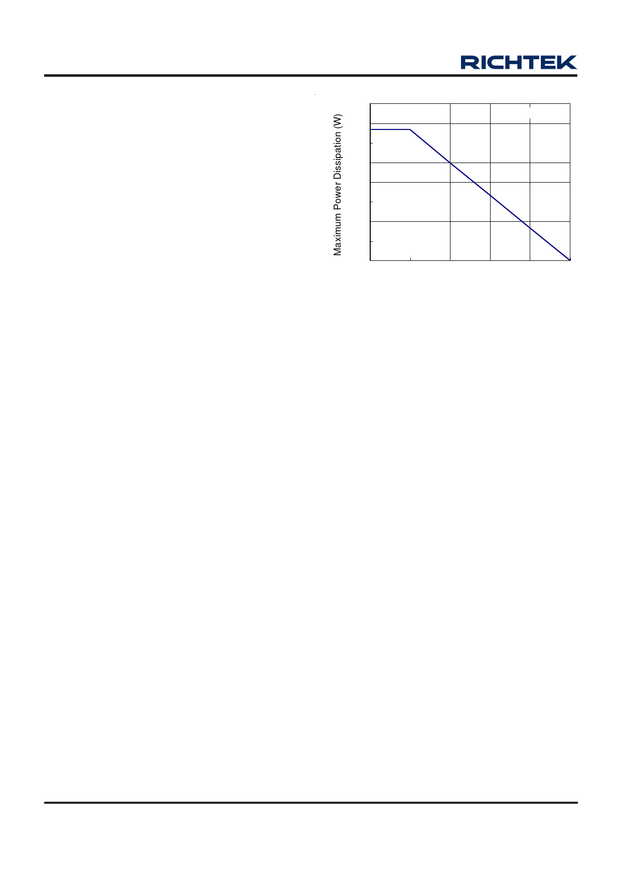
Thermal Considerations
For continuous operation, do not exceed the maximum
operation junction temperature 125°C. The maximum
power dissipation depends on the thermal resistance of
IC package, PCB layout, the rate of surroundings airflow
and temperature difference between junction to ambient.
The maximum power dissipation can be calculated by
following formula :
PD(MAX) = ( TJ(MAX) - TA ) / θJA
Where TJ(MAX) is the maximum operation junction
temperature, TA is the ambient temperature and the θJA is
the junction to ambient thermal resistance.
For recommended operating conditions specification of
RT8269, the maximum junction temperature is 125°C. The
junction to ambient thermal resistance θJA is layout
dependent. For SOP-8 (Exposed Pad) package, the
thermal resistance θJA is 75°C/W on the standard JEDEC
51-7 four-layers thermal test board. The maximum power
dissipation at TA = 25°C can be calculated by following
formula :
PD(MAX) = (125°C − 25°C) / (75°C/W) = 1.333W for
SOP-8 (Exposed Pad) package
The maximum power dissipation depends on operating
ambient temperature for fixed TJ(MAX) and thermal
resistance θJA. For RT8269 package, the Figure 3 of
derating curves allows the designer to see the effect of
rising ambient temperature on the maximum power
dissipation allowed.
1.6
Four Layers PCB
1.4
1.2
1.0
0.8
0.6
0.4
0.2
0.0
0
25
50
75
100
125
Ambient Temperature (°C)
Figure 3. Derating Curve for RT8269 Package
Layout Consideration
Follow the PCB layout guidelines for optimal performance
of RT8269.
` Keep the traces of the main current paths as short and
wide as possible.
` Put the input capacitor as close as possible to the device
pins (VIN and GND).
` LX node is with high frequency voltage swing and should
be kept at small area. Keep analog components away
from the LX node to prevent stray capacitive noise pick-
up.
` Connect feedback network behind the output capacitors.
Keep the loop area small. Place the feedback
components near the RT8269.
` Connect all analog grounds to a command node and
then connect the command node to the power ground
behind the output capacitors.
` An example of PCB layout guide is shown in Figure 4
for reference.
www.richtek.com
10
DS8269-02 March 2011
Share Link: 