RT8286 Ver la hoja de datos (PDF) - Richtek Technology
Número de pieza
componentes Descripción
Fabricante
RT8286 Datasheet PDF : 14 Pages
| |||
RT8286
Application Information
The IC is a synchronous high voltage buck converter that
can support the input voltage range from 4.5V to 21V and
the output current can be up to 2A.
Output Voltage Setting
The output voltage is set by an external resistive divider
according to the following equation :
VOUT
=
VFB
⎛⎜⎝1+
R1
R2
⎞⎟⎠
where VFB is the feedback reference voltage 0.808V
(typical).
The resistive divider allows the FB pin to sense a fraction
of the output voltage as shown in Figure 1.
VOUT
R1
FB
RT8286
R2
GND
Figure 1. Output Voltage Setting
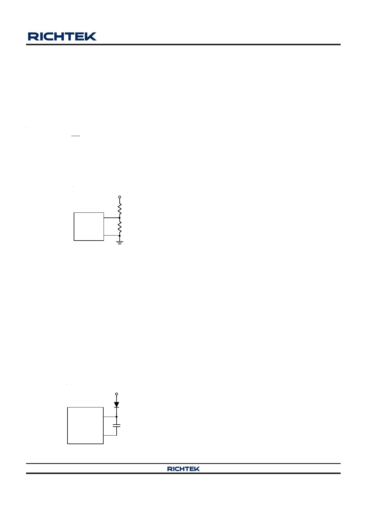
External Bootstrap Diode
Connect a 100nF low ESR ceramic capacitor between
the BOOT pin and SW pin as shown in Figure 2. This
capacitor provides the gate driver voltage for the high side
MOSFET. It is recommended to add an external bootstrap
diode between an external 5V and BOOT pin for efficiency
improvement when input voltage is lower than 5.5V or duty
ratio is higher than 65% .The bootstrap diode can be a
low cost one such as IN4148 or BAT54. The external 5V
can be a 5V fixed input from system or a 5V output of the
IC. Note that the external boot voltage must be lower than
5.5V.
5V
BOOT
RT8286
SW
100nF
Soft-Start
The IC contains an internal soft-start function to prevent
large inrush current and output voltage overshoot when
the converter starts up. Soft-start automatically begins
once the chip is enabled. During soft-start, the internal
soft-start capacitor becomes charged and generates a
linear ramping up voltage across the capacitor. This voltage
clamps the voltage at the internal reference, causing the
duty pulse width to increase slowly and in turn reduce the
output surge current. Finally, the internal 1V reference
takes over the loop control once the internal ramping-up
voltage becomes higher than 1V. The typical soft-start
time for this IC is set at 2ms.
Under Voltage Lockout Threshold
The IC includes an input Under Voltage Lockout Protection
(UVLO). If the input voltage exceeds the UVLO rising
threshold voltage (4.2V), the converter resets and prepares
the PWM for operation. If the input voltage falls below the
UVLO falling threshold voltage (3.8V) during normal
operation, the device stops switching. The UVLO rising
and falling threshold voltage includes a hysteresis to
prevent noise caused reset.
Chip Enable Operation
The EN pin is the chip enable input. Pulling the EN pin
low (<0.4V) will shut down the device. During shutdown
mode, the IC quiescent current drops to lower than 1μA.
Driving the EN pin high (>2V, < 5.5V) will turn on the
device again. For external timing control (e.g.RC), the
EN pin can also be externally pulled high by adding a
REN* resistor and CEN* capacitor from the VIN pin, as can
be seen from the Figure 5.
An external MOSFET can be added to implement digital
control on the EN pin when front age system voltage below
2.5V is available, as shown in Figure 3. In this case, a
100kΩ pull-up resistor, REN, is connected between VIN
and the EN pin. MOSFET Q1 will be under logic control
to pull down the EN pin.
Figure 2. External Bootstrap Diode
Copyright ©2012 Richtek Technology Corporation. All rights reserved.
DS8286-02 June 2012
is a registered trademark of Richtek Technology Corporation.
www.richtek.com
9
Share Link: 