RT8280 Ver la hoja de datos (PDF) - Richtek Technology
Número de pieza
componentes Descripción
Fabricante
RT8280 Datasheet PDF : 16 Pages
| |||
Application Information
The RT8280 is an asynchronous high voltage buck
converter that supports an input voltage range from 4.5V
to 24V with output current up to 3A.
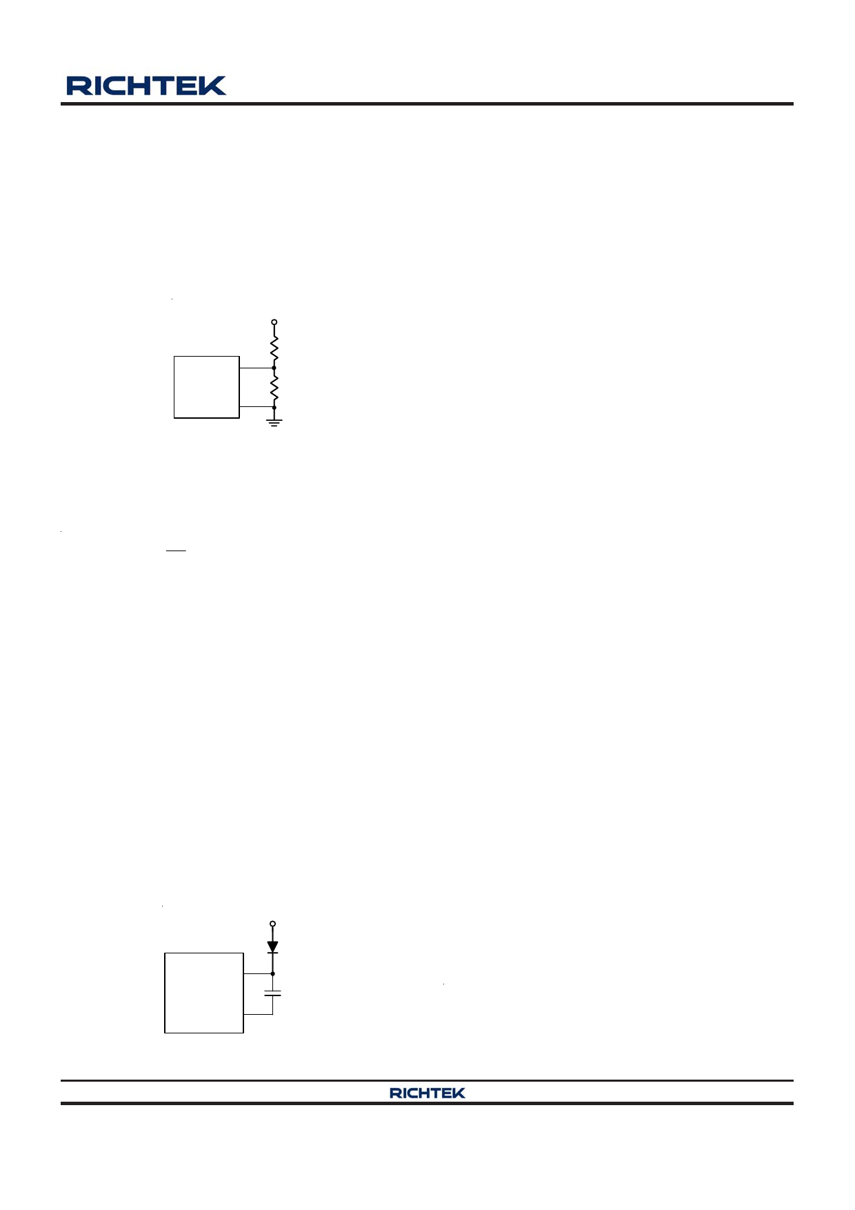
Output Voltage Setting
The resistive voltage divider allows the FB pin to sense
the output voltage as shown in Figure 1.
VOUT
R1
FB
RT8280
R2
GND
Figure 1. Output Voltage Setting
The output voltage is set by an external resistive voltage
divider according to the following equation :
VOUT
=
VFB
⎛⎜⎝1+
R1
R2
⎞⎟⎠
where VFB is the feedback reference voltage (0.8V typ.).
External Bootstrap Diode
Connect a 10nF low ESR ceramic capacitor between the
BOOT pin and SW pin. This capacitor provides the gate
driver voltage for the high side MOSFET.
It is recommended to add an external bootstrap diode
between an external 5V voltage source and the BOOT
pin for efficiency improvement when input voltage is lower
than 5.5V or duty cycle is higher than 65% .The bootstrap
diode can be a low cost one such as IN4148 or BAT54.
The external voltage source must be fixed at 5V and can
be provided from the system or the output of the RT8280.
Note that the external boot voltage must be lower than
5.5V.
5V
BOOT
RT8280
SW
10nF
RT8280
Operating Frequency
Selection of the operating frequency is a trade off between
efficiency and component size. High frequency operation
allows the use of smaller inductor and capacitor values.
Operation at lower frequency improves efficiency by
reducing internal gate charge and switching losses, but
requires larger inductance and/or capacitance to maintain
low output ripple voltage. The operating frequency of the
RT8280 is determined by an external resistor that is
connected between the RT pin and ground. The value of
the resistor sets the ramp current that is used to charge
and discharge an internal timing capacitor within the
oscillator. Selection of the RT resistor value can be
determined by examining the curve below in Figure3.
Although frequencies as high as 3MHz are available, the
minimum on-time of the RT8280 imposes a limit on the
operating duty cycle. Figure 4 shows the examples of
minimum on-time constraint for output voltages 3.3V and
1.8V. It is recommended to operate the RT8280 in the
region under the corresponding Vout curve.
Except the minimum on-time constraint, the limit of
maximum duty also needs to be considered. In ideal case,
the duty cycle of the RT8280 can be calculated by below
equation, But in practical case it will be higher than the
calculation result since all the components in a converter
circuit are not ideal. Figure 5 shows an example for the
limit of maximum duty. With 5V input voltage, the 3.3V
output voltage of the RT8280 becomes out of regulation
when the output current is increased. However, when the
input voltage is changed to 12V, the 3.3V output voltage
of the RT8280 remains in regulation even with 3A output
current. According to equation below, the duty cycle is
0.67 for the RT8280 operated with 5V input voltage and
3.3V output voltage in 2.2MHz switching frequency. The
ideal case duty cycle calculation is already over the limit
of maximum duty (65%). Thus, it is obvious that the
RT8280 can't support 3A output current in such
conditions :
Duty Cycle = 1− 0.15 x fSW (MHz)
Figure 2. External Bootstrap Diode
Copyright ©2012 Richtek Technology Corporation. All rights reserved.
DS8280-02 March 2012
is a registered trademark of Richtek Technology Corporation.
www.richtek.com
9
Share Link: 