RT8074GSP Ver la hoja de datos (PDF) - Richtek Technology
Número de pieza
componentes Descripción
Fabricante
RT8074GSP Datasheet PDF : 10 Pages
| |||
RT8074
Marking Information
RT8074GSP : Product Number
RT8074
YMDNN : Date Code
GSPYMDNN
Functional Pin Description
Pin No.
Pin Name
Pin Function
1
COMP
2,
9 (Exposed Pad)
GND
Error Amplifier Compensation Point. The current comparator threshold increases
with this control voltage. Connect external compensation elements to this pin to
stabilize the control loop.
Ground. The exposed pad must be soldered to a large PCB and connected to GND
for maximum power dissipation.
3
EN
Enable Control Input. Float or connect this pin to logic high for enable. Connect to
GND for disable.
4
VIN
Power Input Supply. Decouple this pin to GND with a capacitor.
5, 6
LX
Internal Power MOSFET Switches Output. Connect this pin to the inductor.
Oscillator Resistor Input. Connecting a resistor from this pin to GND sets the
7
RT
switching frequency. If this pin is floating, the frequency will be set at 2MHz
internally.
8
FB
Feedback. Receives the feedback voltage from a resistive divider connected across
the output.
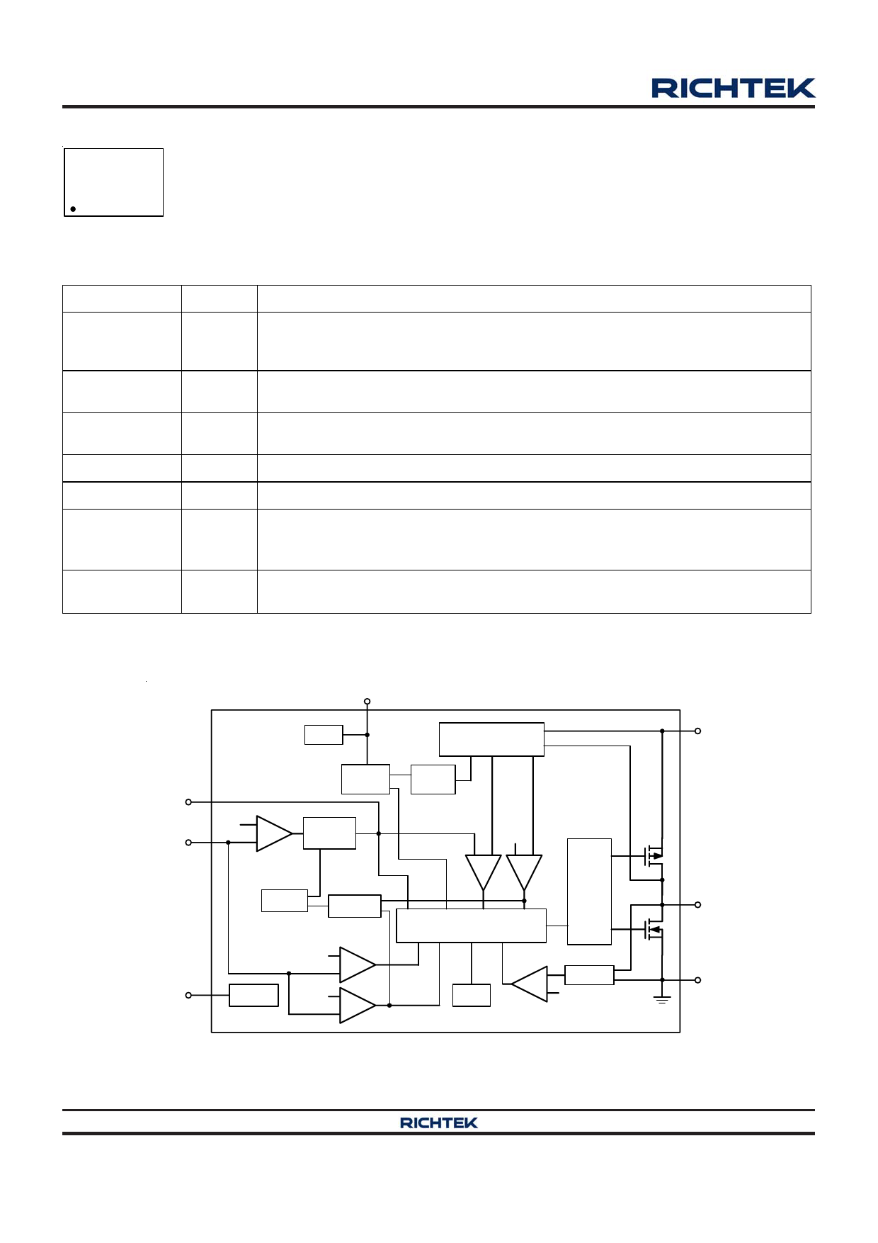
Function Block Diagram
RT
SD
COMP
FB
0.8V
EA
OSC
Output
Clamp
Slope
Com
ISEN
OC
Limit
Int-SS
Hiccup
0.7V
P-G
EN
Enable
0.4V
UV
Control
Logic
OTP
Driver
NISEN
N-MOS ILIM
VIN
LX
GND
Copyright ©2012 Richtek Technology Corporation. All rights reserved.
www.richtek.com
2
is a registered trademark of Richtek Technology Corporation.
DS8074-07 November 2012
Share Link: 