RT8063GSP Ver la hoja de datos (PDF) - Richtek Technology
Número de pieza
componentes Descripción
Fabricante
RT8063GSP Datasheet PDF : 11 Pages
| |||
RT8063
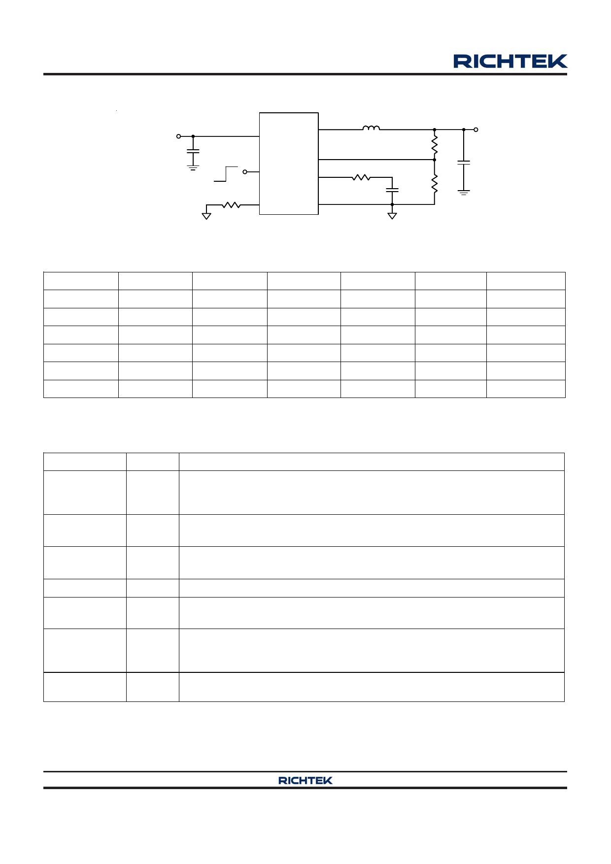
Typical Application Circuit
VIN
2.7V to 5.5V
CIN
10µF
4
RT8063
VIN
LX
5, 6
3 EN
FB 8
COMP 1
L
RCOMP
ROSC 7 RT
GND 2,
9 (Exposed Pad)
R1
R2
CCOMP
Note : Using all Ceramic Capacitors
VOUT
COUT
VOUT (V)
3.3
2.5
1.8
1.5
1.2
1.0
Table 1. Recommended Components Selection for fSW = 1MHz
R1 (kΩ)
R2 (kΩ)
RCOMP (kΩ) CCOMP (pF)
L (μH)
75
24
33
560
2
51
24
22
560
2
30
24
15
560
1.5
21
24
13
560
1.5
12
24
11
560
1.5
6
24
8.2
560
1.5
COUT (μF)
22
22
22
22
22
22
Functional Pin Description
Pin No.
1
Pin Name
Pin Function
Error Amplifier Compensation Point. The current comparator threshold increases
COMP with this control voltage. Connect external compensation elements to this pin to
stabilize the control loop.
2,
GND
9 (Exposed Pad)
Ground. The exposed pad must be soldered to a large PCB and connected to GND
for maximum power dissipation.
Enable Control Input. Float or connect this pin to logic high for enable. Connect to
3
EN
GND for disable.
4
VIN
Power Input Supply. Decouple this pin to GND with a capacitor.
5, 6
LX
7
RT
8
FB
Internal Power MOSFET Switches Output. Connect these pins to the inductor
together.
Oscillator Resistor Input. Connecting a resistor from this pin to GND sets the
switching frequency. If this pin is floating, the frequency will be set at 2MHz
internally.
Feedback. Receives the feedback voltage from a resistive divider connected across
the output.
Copyright ©2012 Richtek Technology Corporation. All rights reserved.
www.richtek.com
2
is a registered trademark of Richtek Technology Corporation.
DS8063-07 November 2012
Share Link: 