RT8063GSP Ver la hoja de datos (PDF) - Richtek Technology
Número de pieza
componentes Descripción
Fabricante
RT8063GSP Datasheet PDF : 11 Pages
| |||
RT8063
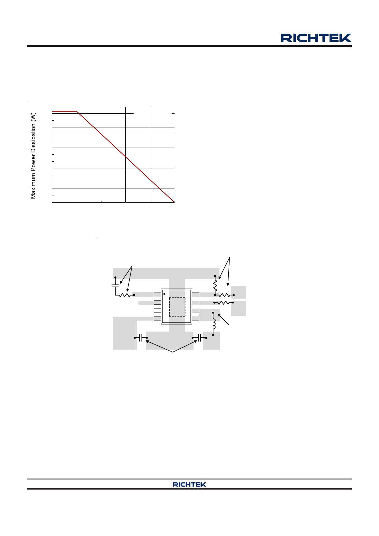
The maximum power dissipation depends on the operating
ambient temperature for fixed TJ(MAX) and thermal
resistance, θJA. The derating curve in Figure 3 allows the
designer to see the effect of rising ambient temperature
on the maximum power dissipation.
1.4
1.3
1.2
1.1
1.0
0.9
0.8
0.7
0.6
0.5
0.4
0.3
0.2
0.1
0.0
0
Four-Layer PCB
25
50
75
100
125
Ambient Temperature (°C)
Figure 3. Derating Curve of Maximum Power Dissipation
Layout Considerations
Follow the PCB layout guidelines for optimal performance
of the IC.
` Connect the terminal of the input capacitor(s), CIN, as
close as possible to the VIN pin. This capacitor provides
the AC current into the internal power MOSFETs.
` LX node experiences high frequency voltage swing and
should be kept within a small area.
` Keep all sensitive small-signal nodes away from the LX
node to prevent stray capacitive noise pick up.
` Connect the FB pin directly to the feedback resistors.
The resistive voltage divider must be connected between
VOUT and GND.
Place the compensation
components as close to
the IC as possible
Place the feedback
resistors as close to the
IC as possible
GND
CCOMP
COMP
R2
R1 VOUT
8 FB
RCOMP
GND
EN
VIN
VIN
CIN
2
7 RT
GND
3
96
LX
4
5 LX
COUT
ROSC
GND
L1
LX should be connected
to inductor by wide and
short trace, and keep
VOUT sensitive components
Place the input and output capacitors
away from this trace
as close to the IC as possible
Figure 4. PCB Layout Guide
Copyright ©2012 Richtek Technology Corporation. All rights reserved.
www.richtek.com
10
is a registered trademark of Richtek Technology Corporation.
DS8063-07 November 2012
Share Link: 