RT8026 Ver la hoja de datos (PDF) - Richtek Technology
Número de pieza
componentes Descripción
Fabricante
RT8026 Datasheet PDF : 12 Pages
| |||
RT8026
losses are proportional to VIN and thus their effects will
be more pronounced at higher supply voltages.
2. I2R losses are calculated from the resistances of the
internal switches, RSW and external inductor RL. In
continuous mode the average output current flowing
through inductor L is “chopped” between the main switch
and the synchronous switch. Thus, the series resistance
looking into the LX pin is a function of both top and bottom
MOSFET RDS(ON) and the duty cycle (DC) as follows :
RSW = RDS(ON)TOP x DC + RDS(ON)BOT x (1−DC)
The RDS(ON) for both the top and bottom MOSFETs can be
obtained from the Typical Performance Characteristics
curves. Thus, to obtain I2R losses, simply add RSW to RL
and multiply the result by the square of the average output
current.
Other losses including CIN and COUT ESR dissipative
losses and inductor core losses generally account for less
than 2% of the total loss.
Thermal Considerations
For continuous operation, do not exceed absolute
maximum operation junction temperature. The maximum
power dissipation depends on the thermal resistance of
IC package, PCB layout, the rate of surroundings airflow
and temperature difference between junction to ambient.
The maximum power dissipation can be calculated by
following formula :
PD(MAX) = ( TJ(MAX) − TA ) / θJA
Where TJ(MAX) is the maximum operation junction
temperature 125°C, TA is the ambient temperature and
the θJAis the junction to ambient thermal resistance.
For recommended operating conditions specification of
RT8026, the maximum junction temperature is 125°C.The
junction to ambient thermal resistance θJA is layout
dependent. For MSOP-10 packages, the thermal
resistance θJA is 120°C/W on the standard JEDEC 51-7
four layers thermal test board. The maximum power
dissipation at TA = 25°C can be calculated by following
formula :
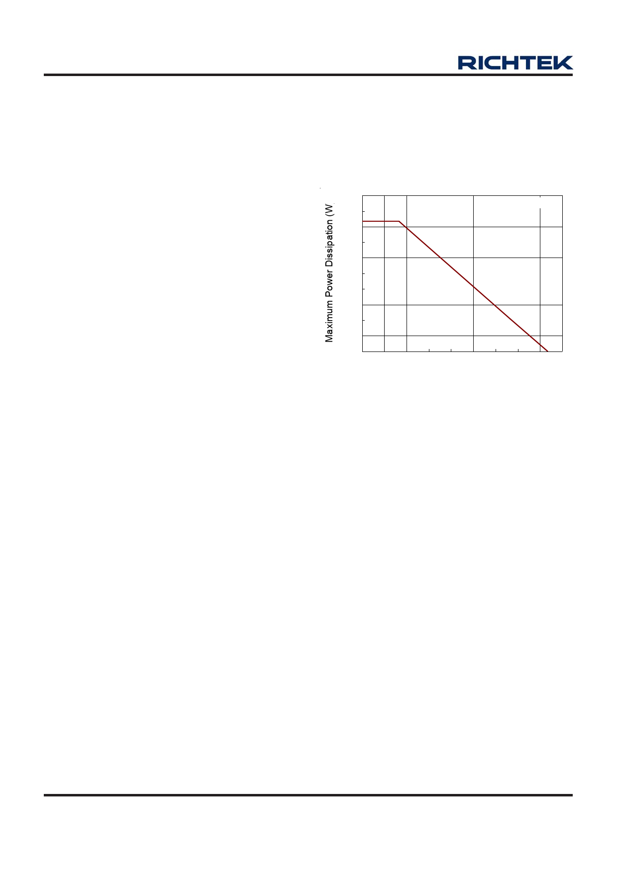
PD(MAX) = (125°C − 25°C) / (120°C/W) = 0.833W for
MSOP-10 packages
The maximum power dissipation depends on operating
ambient temperature for fixed TJ(MAX) and thermal
resistance θJA. For RT8026 packages, the Figure 3 of
derating curves allows the designer to see the effect of
rising ambient temperature on the maximum power
allowed.
1.0
0.9
0.8
0.7
0.6
0.5
0.4
0.3
0.2
0.1
0.0
0
Four Layers PCB
15 30 45 60 75 90 105 120 135
Ambient Temperature (°C)
Figure 3. Derating Curves for RT8026 Packages
Layout Considerations
For the best performance of the RT8026, the following
guidelines must be strictly followed.
` The input capacitor should be placed as close as possible
to the device pins (VIN and GND).
` The LX node is with high frequency voltage swing. It
should be kept at a small area.
` Place the feedback components as close as possible to
the IC and keep away from the noisy devices.
` The GND and PGND should be connected to a strong
ground plane for heat sinking and noise protection.
www.richtek.com
10
DS8026-02 March 2011
Share Link: 