1112IB Ver la hoja de datos (PDF) - Intersil
Número de pieza
componentes Descripción
Fabricante
1112IB Datasheet PDF : 14 Pages
| |||
HFA1112
Absolute Maximum Ratings
Voltage Between V+ and V- . . . . . . . . . . . . . . . . . . . . . . . . . . . . .12V
Input Voltage . . . . . . . . . . . . . . . . . . . . . . . . . . . . . . . . . . . VSUPPLY
Output Current . . . . . . . . . . . . . . . . . . . . . . . . . . . . . . . . . . . . . 60mA
Operating Conditions
Temperature Range . . . . . . . . . . . . . . . . . . . . . . . . . . -40oC to 85oC
Thermal Information
Thermal Resistance (Typical, Note 1)
θJA (oC/W) θJC (oC/W)
PDIP Package . . . . . . . . . . . . . . . . . . . 125
N/A
SOIC Package . . . . . . . . . . . . . . . . . . . 170
N/A
Maximum Junction Temperature (Plastic Package) . . . . . . . .150oC
Maximum Storage Temperature Range . . . . . . . . . . -65oC to 150oC
Maximum Lead Temperature (Soldering 10s) . . . . . . . . . . . . 300oC
(SOIC - Lead Tips Only)
CAUTION: Stresses above those listed in “Absolute Maximum Ratings” may cause permanent damage to the device. This is a stress only rating and operation of the
device at these or any other conditions above those indicated in the operational sections of this specification is not implied.
NOTE:
1. θJA is measured with the component mounted on a low effective thermal conductivity test board in free air. See Tech Brief TB379 for details.
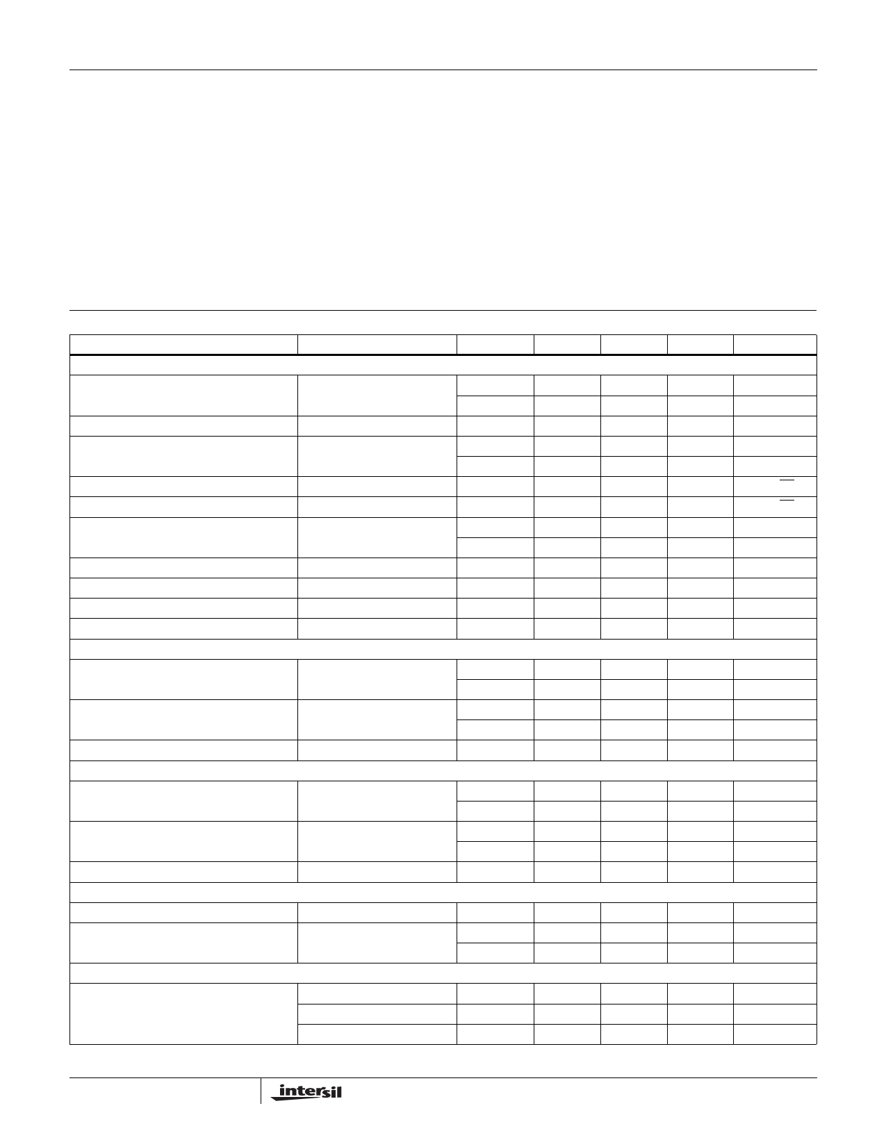
Electrical Specifications VSUPPLY = ±5V, AV = +1, RL = 100Ω, Unless Otherwise Specified
PARAMETER
TEST CONDITIONS
TEMP (oC)
MIN
INPUT CHARACTERISTICS
Output Offset Voltage
25
-
Full
-
Output Offset Voltage Drift
Full
-
PSRR
25
39
Full
35
Input Noise Voltage (Note 3)
100kHz
25
-
Non-Inverting Input Noise Current (Note 3) 100kHz
25
-
Non-Inverting Input Bias Current
25
-
Full
-
Non-Inverting Input Resistance
25
25
Inverting Input Resistance (Note 2)
25
240
Input Capacitance
25
-
Input Common Mode Range
Full
±2.5
TRANSFER CHARACTERISTICS
Gain
AV = +1, VIN = +2V
25
0.980
Full
0.975
Gain
AV = +2, VIN = +1V
25
1.96
Full
1.95
DC Non-Linearity (Note 3)
OUTPUT CHARACTERISTICS
AV = +2, ±2V Full Scale
25
-
Output Voltage (Note 3)
AV = -1
25
±3.0
Full
±2.5
Output Current (Note 3)
RL = 50Ω
25, 85
50
-40
35
Closed Loop Output Impedance
POWER SUPPLY CHARACTERISTICS
DC, AV = +2
25
-
Supply Voltage Range
Full
±4.5
Supply Current (Note 3)
25
-
Full
-
AC CHARACTERISTICS
-3dB Bandwidth
(VOUT = 0.2VP-P, Notes 2, 3)
AV = -1
AV = +1
AV = +2
25
450
25
500
25
350
TYP
8
-
10
45
-
9
37
25
-
50
300
2
±2.8
0.990
-
1.98
-
0.02
±3.3
±3.0
60
50
0.3
-
21
-
800
850
550
MAX
25
35
-
-
-
-
-
40
65
-
360
-
-
1.02
1.025
2.04
2.05
-
-
-
-
-
-
±5.5
26
33
-
-
-
UNITS
mV
mV
µV/oC
dB
dB
nV/√Hz
pA/√Hz
µA
µA
kΩ
Ω
pF
V
V/V
V/V
V/V
V/V
%
V
V
mA
mA
Ω
V
mA
mA
MHz
MHz
MHz
2
Share Link: 