HIP4086(2015) Ver la hoja de datos (PDF) - Intersil
Número de pieza
componentes Descripción
Fabricante
HIP4086 Datasheet PDF : 16 Pages
| |||
HIP4086, HIP4086A
Charge Pump
The internal charge pump of the HIP4086/A is used to maintain
the bias on the boot cap for 100% duty cycle. There is no limit for
the duration of this period. The user must understand that this
charge pump is only intended to provide the static bias current of
the high-side drivers and the gate leakage current of the
high-side bridge FETs. It cannot provide in a reasonable time, the
majority of the charge on the boot cap that is consumed, when
the xHO drivers source the gate charge to turn on the high-side
bridge FETs. The boot caps should be sized so that they do not
discharge excessively when sourcing the gate charge. See
“Application Information” on page 11 for methods to size the
boot caps.
The charge pump has sufficient capacity to source a worst-case
minimum of 50µA to the external load. The gate leakage current
of most power MOSFETs is about 100nA so there is more than
sufficient current to maintain the charge on the boot caps.
Because the charge pump current is small, a gate-source resistor
on the high-side bridge FETs is not recommended. When
calculating the leakage load on the outputs of xHS, also include
the leakage current of the boot capacitor. This is rarely a problem
but it could be an issue with electrolytic capacitors at high
temperatures.
Application Information
Selecting the Boot Capacitor Value
The boot capacitor value is chosen not only to supply the internal
bias current of the high-side driver but also, and more
significantly, to provide the gate charge of the driven FET without
causing the boot voltage to sag excessively. In practice, the boot
capacitor should have a total charge that is about 20 times the
gate charge of the driven power FET for approximately a 5% drop
in voltage after charge has been transferred from the boot
capacitor to the gate capacitance.
The following parameters shown in Table 1 are required to
calculate the value of the boot capacitor for a specific amount of
voltage droop when using the HIP4086/A (no charge pump). In
Table 1, the values used are arbitrary. They should be changed to
comply with the actual application.
TABLE 1.
VDD = 10V
VHB = VDD - 0.6V
= VHO
Period = 1ms
VDD can be any value between 7 and 15VDC.
High-side driver bias voltage (VDD - boot diode
voltage) referenced to VHS.
This is the longest expected switching period.
IHB= 100µA
Worst case high-side driver current when
xHO = high (this value is specified for VDD = 12V
but the error is not significant).
RGS = 100kΩ
Ripple = 5%
Gate-source resistor (usually not needed).
Desired ripple voltage on the boot cap (larger
ripple is not recommended).
Igate_leak = 100nA
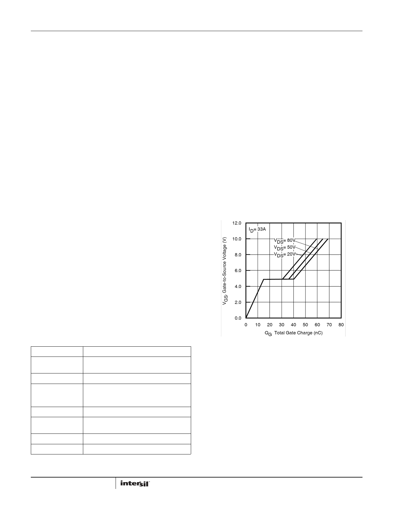
Qgate80V = 64nC
From the FET vendor’s datasheet.
From Figure 21.
Equation 1 calculates the total charge required for the Period
duration. This equation assumes that all of the parameters are
constant during the Period duration. The error is insignificant if
Ripple is small.
QC = Qgate80V + Period (IHB + VHO RGS + Igate_leak)
Cboot = QC RippleVDD
Cboot = 0.52F
(EQ. 1)
If the gate to source resistor is removed (RGS is usually not
needed or recommended), then:
Cboot = 0.33µF
These values of Cboot will sustain the high side driver bias during
Period with only a small amount of Ripple. But in the case of the
HIP4086, the charge pump reduces the value of Cboot even
more. The specified charge pump current is a minimum of 50µA
which is more than sufficient to source Igate_leak. Also, because
the specified charge pump current is in excess of what is needed
for IHB, the total charge required to be sourced by the boot
capacitor is shown by Equation 2.
QC = Qgate80Vor Cboot = 0.13F
(EQ. 2)
Not only is the required boot cap smaller in value, there is no
restriction on the duration of Period.
FIGURE 21. TYPICAL GATE VOLTAGE vs GATE CHARGE
Submit Document Feedback 11
FN4220.10
March 27, 2015
Share Link: 