RF3806 Ver la hoja de datos (PDF) - RF Micro Devices
Número de pieza
componentes Descripción
Fabricante
RF3806 Datasheet PDF : 18 Pages
| |||
RF3806
Pin Function Description
Interface Schematic
1
VCC1
For input stage.
2
VREF
Control for active bias. See “Theory of Operation” section.
3
RF IN
For input stage. Requires RF match and DC block.
3
4
VBIAS
Supply for active bias.
5
RF OUT/ For output stage. Requires RF match, bias feed and DC block.
VCC2
6
RF OUT/ See pin 5.
VCC2
7
RF OUT/ See pin 5.
VCC2
8
RF OUT/ See pin 5.
VCC2
Pkg
Base
GND
Must be soldered to ground pad through as short a path as possible. This
path also forms the thermal path for minimum TJ.
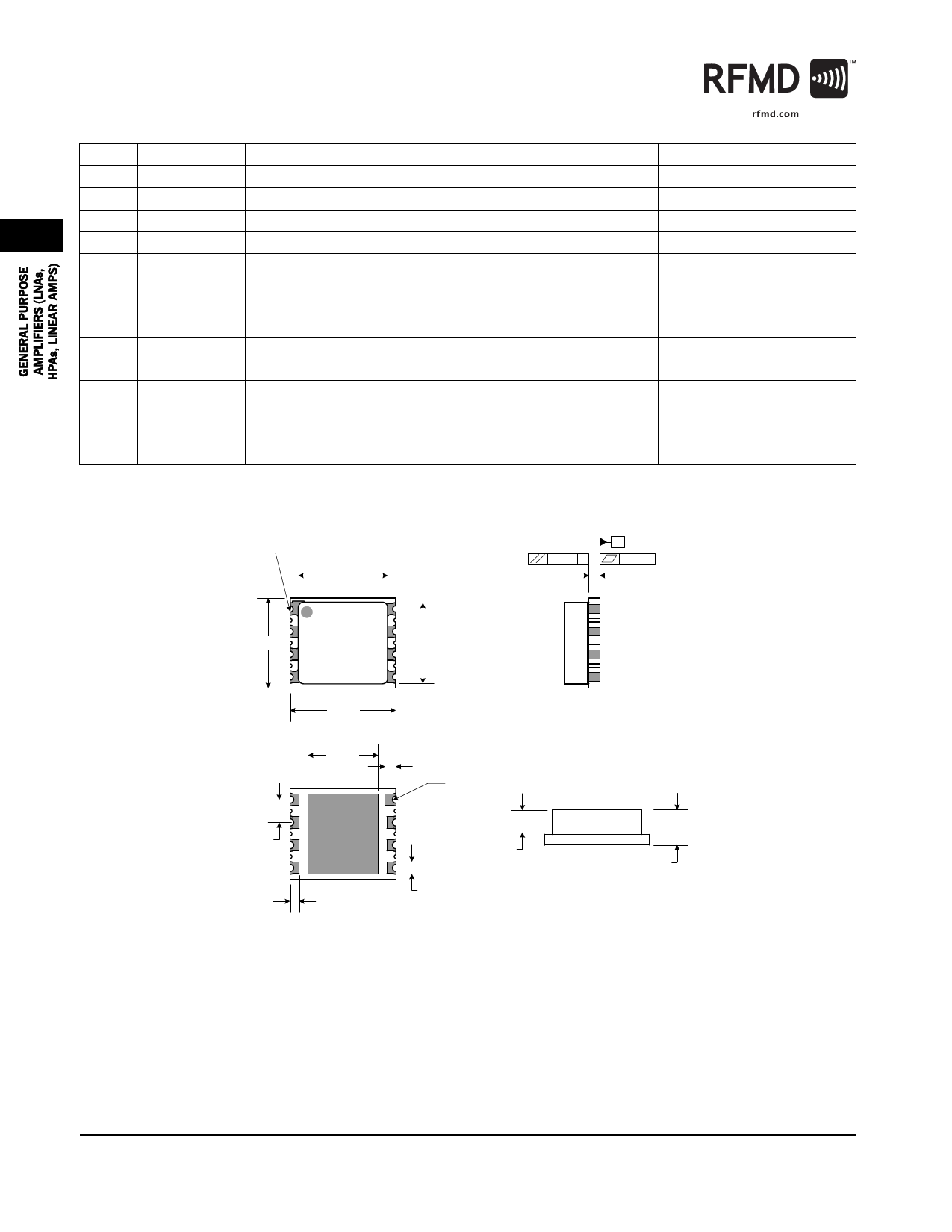
Pin 1
Package Drawing
0.200 REF
Shaded circle designates
pin 1 location.
0.005 A
-A-
0.0025
0.024
0.198
0.180
REF
0.050
TYP
0.020
7 PL
0.236
0.156
Dimensions in inches.
0.025
R.008
0.028
TYP
0.050
REF
0.0780
MAX
3-116
7628 Thorndike Road, Greensboro, NC 27409-9421 · For sales or technical
support, contact RFMD at (+1) 336-678-5570 or sales-support@rfmd.com.
Rev A3 DS070509
Share Link: 