RF3802PCBA-411 Ver la hoja de datos (PDF) - RF Micro Devices
Número de pieza
componentes Descripción
Fabricante
RF3802PCBA-411 Datasheet PDF : 12 Pages
| |||
RF3802
PCB Design Requirements
PCB Surface Finish
The PCB surface finish used for RFMD's qualification process is electroless nickel, immersion gold. Typical thickness is 3μinch
to 8μinch gold over 180μinch nickel.
PCB Land Pattern Recommendation
PCB land patterns for PFMD components are based on IPC-7351 standards and RFMD empirical data. The pad pattern shown
has been developed and tested for optimized assembly at RFMD. The PCB land pattern has been developed to accommodate
lead and package tolerances. Since surface mount processes vary from company to company, careful process development is
recommended.
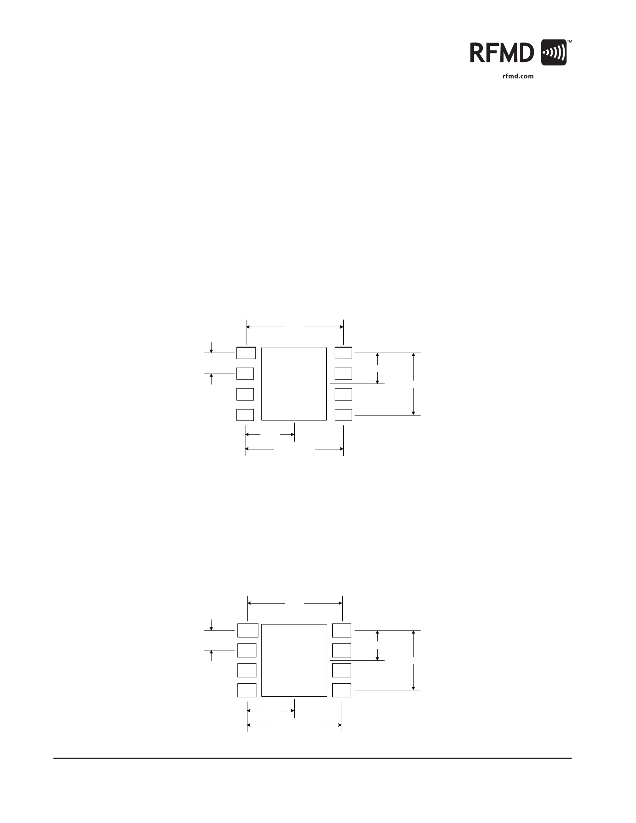
PCB Metal Land Pattern
A = 1.14 x 0.71
B = 1.02 x 0.71 Typ.
C = 3.96 x 4.44
Dimensions in
mm.
5.93
Pin 1
A
B
1.27 Typ.
B
B 1.90
C
3.81 Typ.
B
B
B
B
3.00
5.99 Typ.
PCB Solder Mask Pattern
Liquid Photo-Imageable (LPI) solder mask is recommended. The solder mask footprint will match what is shown for the PCB
metal land pattern with a 2mil to 3mil expansion to accommodate solder mask registration clearance around all pads. The
center-grounding pad shall also have a solder mask clearance. Expansion of the pads to create solder mask clearance can be
provided in the master data or requested from the PCB fabrication supplier.
A = 1.30 x 0.86
B = 1.17 x 0.86 Typ.
C = 4.11 x 4.60
Dimensions in
mm.
5.93
Pin 1
A
B
1.27 Typ.
B
B
1.90
C
3.81 Typ.
B
B
B
B
3.00
5.99 Typ.
10 of 12
7628 Thorndike Road, Greensboro, NC 27409-9421 · For sales or technical
support, contact RFMD at (+1) 336-678-5570 or sales-support@rfmd.com.
Rev A6 DS050609
Share Link: 