RF3166D Ver la hoja de datos (PDF) - RF Micro Devices
Número de pieza
componentes Descripción
Fabricante
RF3166D Datasheet PDF : 14 Pages
| |||
RF3166D
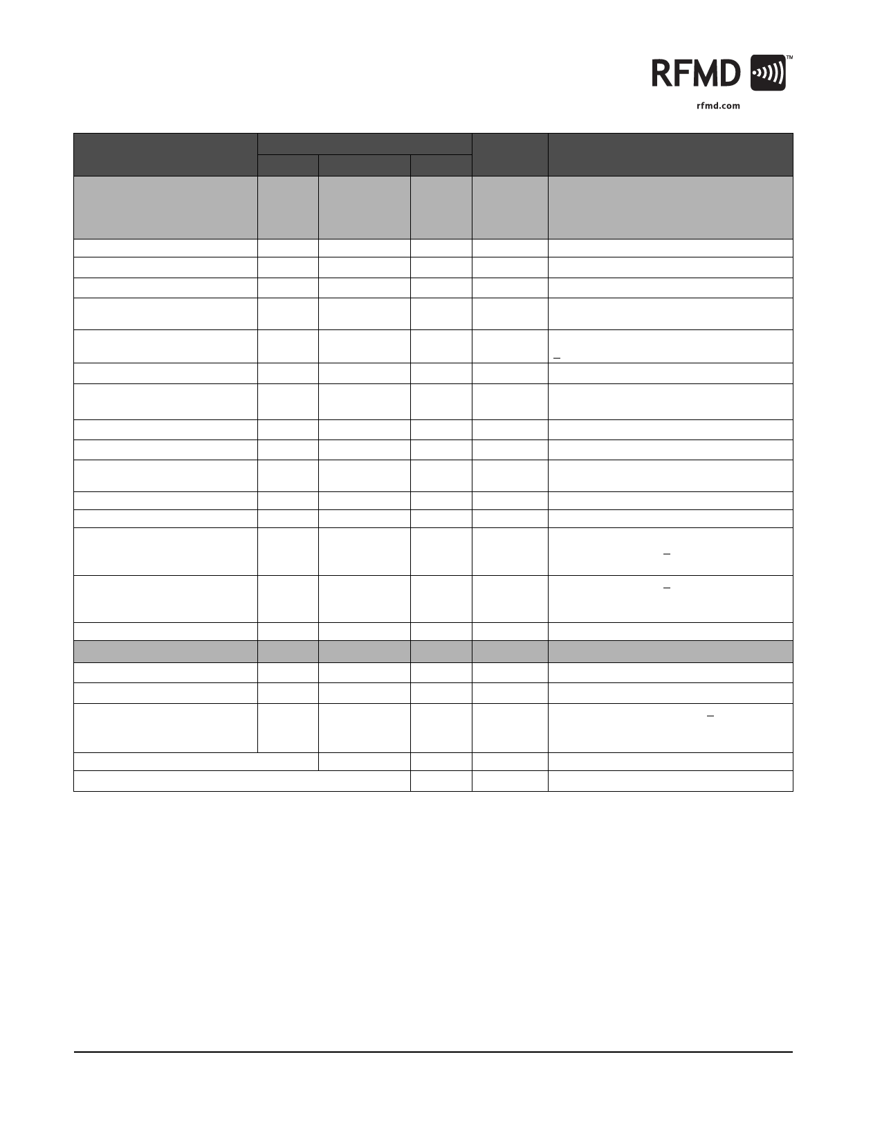
Parameter
Overall (DCS Mode)
Operating Frequency Range
Maximum Output Power 1
Total Efficiency
Input Power Range
Output Noise Power
Forward Isolation 1
Forward Isolation 2
Second Harmonic
Third Harmonic
All Other
Non-Harmonic Spurious
Input Impedance
Input VSWR
Output Load VSWR Stability
Specification
Min.
Typ.
Max.
1710 to 1785
31.5
44
0
+3
+5
-85
-80
-40
-30
-25
-10
-15
-7
-30
-15
-36
50
2.5:1
8:1
Output Load VSWR Ruggedness
10:1
Output Load Impedance
Power Control VRAMP
Power Control Range
Transient Spectrum
Transient Spectrum Under
Extreme Conditions
50
45
50
-35
-23
Notes:
VRAMP_RP=VRAMP set for 31.5dBm at nominal conditions.
Unit
MHz
dBm
%
dBm
dBm
dBm
dBm
dBm
dBm
dBm
Ω
Ω
Condition
Temp=25°C, VBATT=3.5V,
VRAMP=2.1V, PIN=3dBm,
Freq=1710MHz to 1785MHz,
25% Duty Cycle, pulse width=1154μs
Temp=+25°C, VBATT=3.5V, VRAMP=2.1V
At POUT MAX, VBATT=3.5V
Maximum output power guaranteed at mini-
mum drive level
RBW=100kHz, 1805MHz to 1880MHz, POUT
< 31.5dBm
TXEnable=Low, PIN=+5dBm
TXEnable=High, VRAMP=0.26V,
PIN = +5 dBm
VRAMP=0.26V to VRAMP_RP
VRAMP=0.26V to VRAMP_RP
VRAMP=0.26V to 2.1V
Spurious<-36dBm, RBW=3MHz
Set VRAMP where POUT<31.5dBm into 50Ω
load
Set VRAMP where POUT<31.5dBm into 50Ω
load. No damage or permanent degradation to
part.
Load impedance presented at RF OUT pad
dB
dBm
dBm
VRAMP=0.26V to 2.1V
VRAMP = VRAMP_RP
Temp=-20°C to +85°C, VBATT>3.0V.
Ramping shape same as for Condition:
Temp=25°C, VBATT=3.5V, VRAMP=VRAMP_RP
4 of 14
7628 Thorndike Road, Greensboro, NC 27409-9421 · For sales or technical
support, contact RFMD at (+1) 336-678-5570 or sales-support@rfmd.com.
Rev A2 061006
Share Link: 