RF3146D Ver la hoja de datos (PDF) - RF Micro Devices
Número de pieza
componentes Descripción
Fabricante
RF3146D Datasheet PDF : 16 Pages
| |||
RF3146D
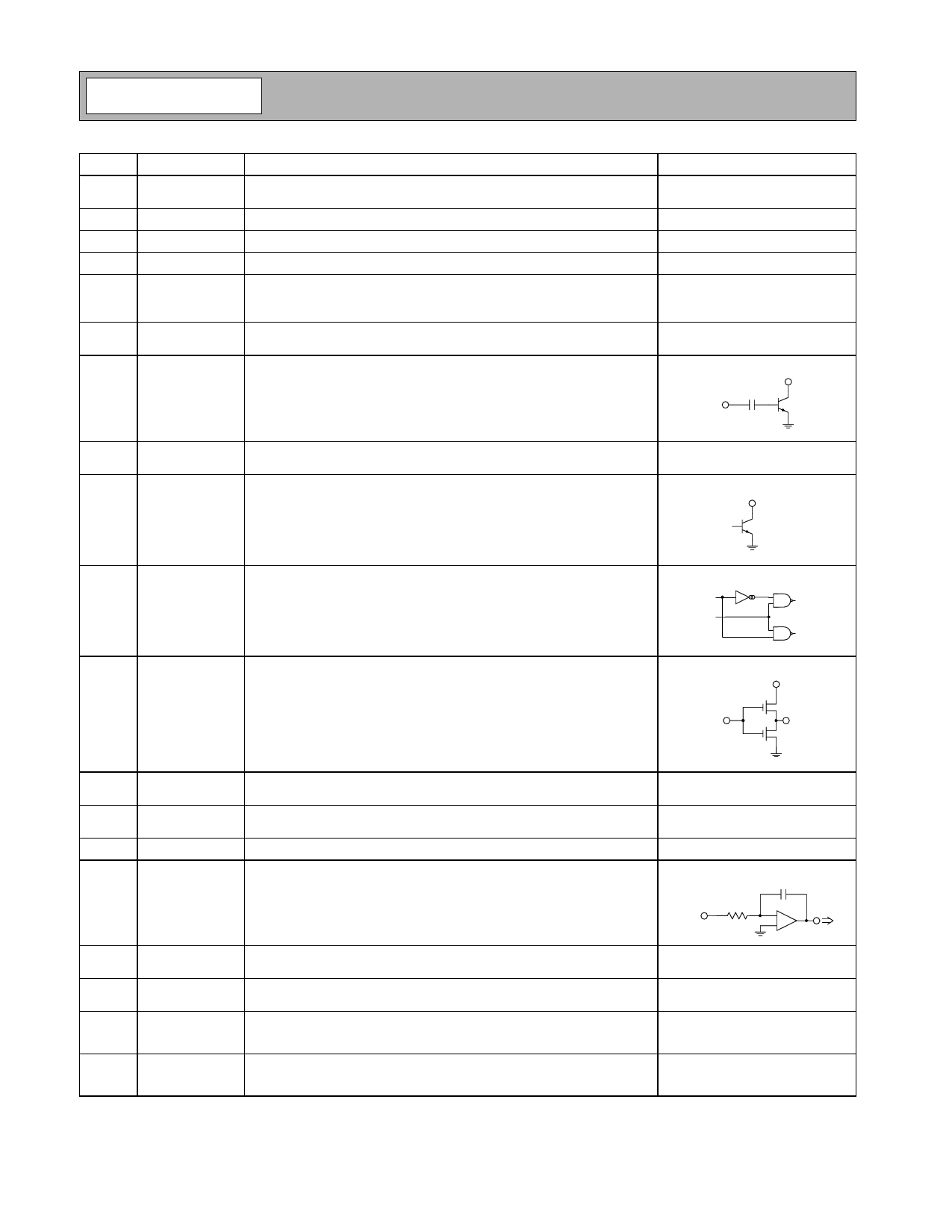
Pin Function Description
Interface Schematic
31
DCS OUT RF output for the DCS band. This is a 50Ω output. The output matching See pin 6.
circuit and DC-block are internal to the package.
32
GND
Internally connected to the package base.
33
NC
Internal circuit node. Do not externally connect.
34
GND
Internally connected to the package base.
35 VCC2 DCS Controlled voltage input to the DCS driver stage. This voltage is part of See pin 2.
the power control function for the module. This node must be con-
nected to VCC OUT. This pin should be externally decoupled.
36
NC
No internal connection. Connect to ground plane close to the package
pin.
37
DCS IN RF input to the DCS band. This is a 50Ω output.
VCC1
RF IN
38
NC
No internal connection. Connect to ground plane close to the package
pin.
39 VCC1 DCS Controlled voltage on the GSM and DCS preamplifier stages. This volt-
age is applied internal to the package. This pin should be externally
VCC1
decoupled.
40 BAND SEL Allows external control to select the GSM or DCS bands with a logic
high or low. A logic low enables the GSM bands, whereas a logic high
enables the DCS/PCS bands.
BAND SEL
TX EN
41 TX ENABLE This signal enables the PA module for operation with a logic high. Both
bands are disabled with a logic low.
TX EN
GSM CTRL
DCS CTRL
VBATT
TX ON
42
VBATT
Power supply for the module. This pin should be externally decoupled
and connected to the battery.
43
VBATT
Power supply for the module. This pin should be externally decoupled
and connected to the battery.
44
NC
Internal circuit node. Do not externally connect.
45
VRAMP Ramping signal from DAC. A simple RC filter may be required depend-
ing on the selected baseband.
VRAMP
-
+
46
47
48
Pkg
Base
VCC1 GSM
GND1 GSM
GSM850/
GSM900 IN
GND
Internally connected to VCC1 (pin 39). No external connection
required.
Ground connection for the GSM preamplifier stage. Connect to ground
plane close to the package pin.
RF input to the GSM band. This is a 50Ω input.
Connect to ground plane with multiple via holes. See recommended
footprint.
See pin 39.
See pin 37.
2-496
Rev A11 060719
Share Link: 