RF2152 Ver la hoja de datos (PDF) - RF Micro Devices
Número de pieza
componentes Descripción
Fabricante
RF2152 Datasheet PDF : 12 Pages
| |||
RF2152
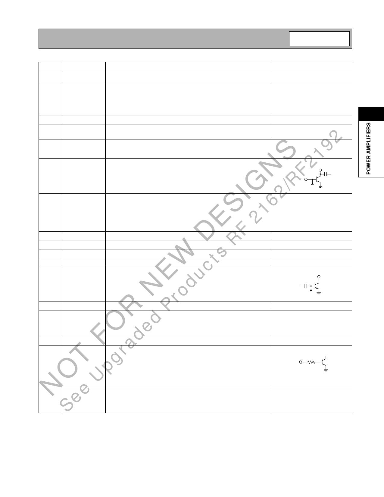
Pin Function Description
Interface Schematic
1
VCC
Power supply for input bias circuitry. A 100 pF high frequency bypass
capacitor is recommended.
2
LTUNE
Interstage tuning. This pin will connect to a shunt inductor used for
interstage tuning. For 824MHz to 849MHz a 1.5nH discrete inductor is
used; for 877MHz to 925MHz a shorted transmission line presenting
0.7 nH of inductance or discrete inductor may be used. This inductor
should be placed as close to the pin as possible.
2
3
NC
No connection. Grounding pin is recommended.
4
VCC1
Power supply for stage 1. VCC should be fed through a 25nH or greater See pin 6.
inductor with a decoupling capacitor on the VCC side.
2 5
GND1
Ground for stage 1. Keep traces physically short and connect immedi- See pin 6.
ately to ground plane for best performance. This ground should be iso-
9 lated from the backside ground contact.
S 1 6
RF IN
RF input. An external DC blocking capacitor is required if this port is
VCC1
2 connected to a DC path to ground or a DC voltage.
N FRF IN
IG 2/R 7
VPD
Power Down control. When this pin is “low”, all circuits are shut off.
When this pin is 2.8 volts, all circuits are operating normally. VPD
6 requires a regulated 2.8 V for the amplifier to operate properly over all
S 1 specified temperature and voltage ranges. A dropping resistor from a
higher regulated voltage may be used to provide the required 2.8 V. A
E 2 100 pF high frequency bypass capacitor is recommended.
F 8
VPD
Connect to pin 7.
From Bias
Stages GND1
D R 9
NC
No connection. Grounding pin is recommended.
10
NC
No connection. Grounding pin is recommended.
W ts 11
NC
No connection. Grounding pin is recommended.
c 12
RF OUT RF output and power supply for the output stage. The bias for the out-
put stage is provided through this pin and pin 13. An external matching
E u network is required to provide the optimum load impedance; see the
d application schematics for details. The first shunt cap of the matching
N o circuit should be placed as close to the pin as possible.
RF OUT
From Bias
Stages
r 13
RF OUT Same as pin 12.
See pin 12.
P 14
RF OUT Harmonic trap. This pin connects to the RF output but is used for pro- See pin 12.
R viding a low impedance to the second harmonic of the operating fre-
d quency. An inductor or transmission line resonating with a shunt
O e capacitor at 2f0 is connected to this pin.
d 15
NC
No connection. Grounding pin is recommended.
F a 16
MODE
The mode pin allows higher efficiency operation in AMPS and low
r power CDMA modes. MODE should be set “low” for highest efficiency
in AMPS/TACS and in low power (<+15 dBm) CDMA operation. MODE
MODE
T gshould be set “high” for best linearity in high power CDMA operation.
O Up Pkg
NSee Base
GND
Ground connection. The backside of the package should be soldered to
a top side ground pad which is connected to the ground plane with mul-
tiple vias. The pad should have a short thermal path to the ground
plane.
Rev A8 001109
2-157
Share Link: 