RA8860 Ver la hoja de datos (PDF) - RAIO
Número de pieza
componentes Descripción
Fabricante
RA8860 Datasheet PDF : 7 Pages
| |||
Version 1.1
RA8860
80x2 Dots 16-Color LCD Driver
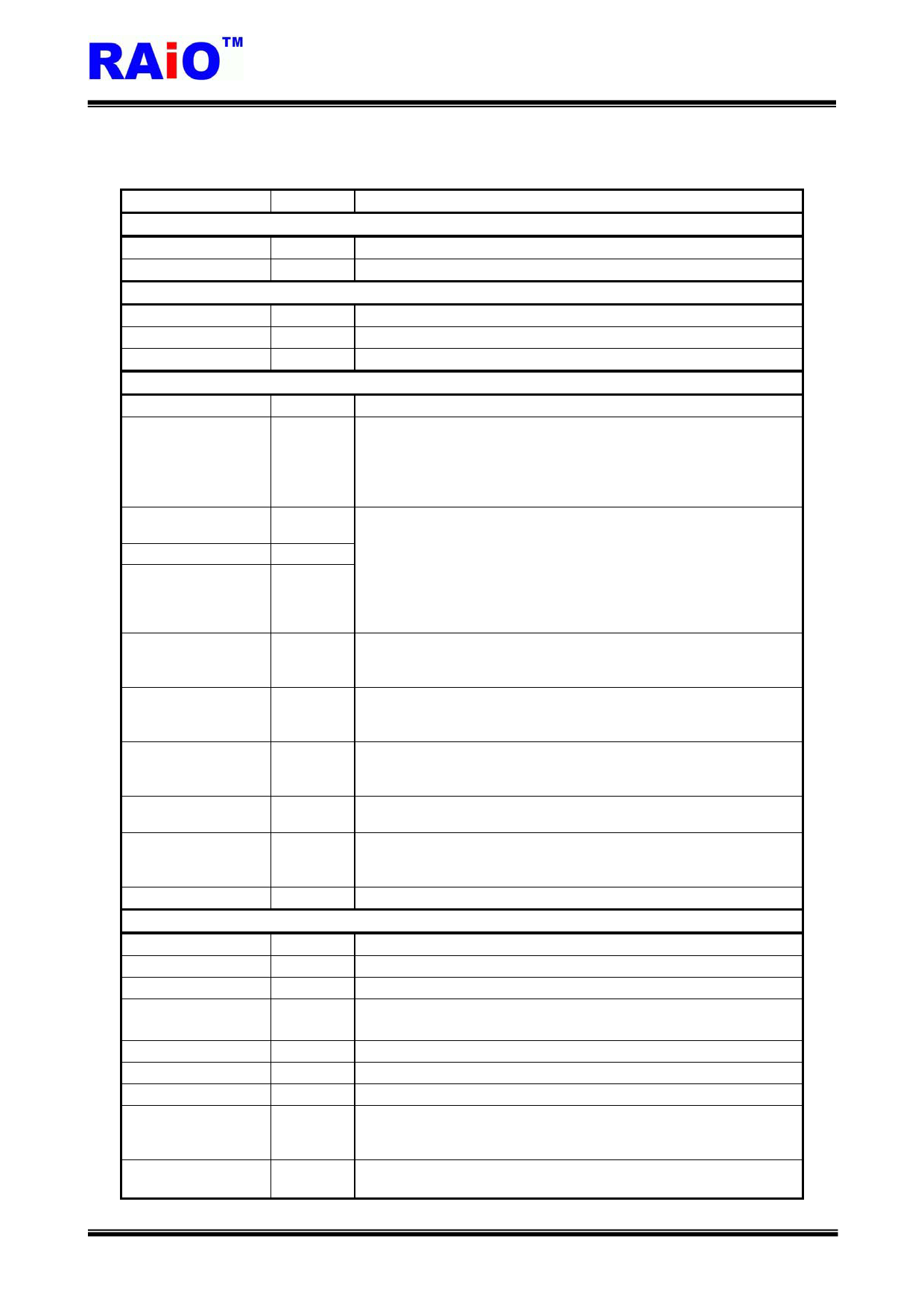
Pin Name
I/O
LCD Driver Outputs
SEG[79:0]
O
COM[1:0]
O
LED Driver Outputs
LED-R
O
LED-G
O
LED-B
O
MCU Interface
/RST
I
IF_SEL[1:0]
I
SCL,
/CS
I
SDA_SDO
I/O
RS_SDI
I
CLK_SEL
I
CL
I
MS
I
SA[2:0]
I
SYNC
I/O
CLK_OUT
O
Power Supply
VDD, GND
P
AVDD, AGND
P
VDDP, GNDP
P
C[3:1]P
C[2:1]N
O
VOUT
P
VREF
P
VR
I
V0
VCM_IN
P
VCM
TP[6:0]
I
8. Pin Description
Description
LCD Segment Driver Outputs.
LCD Common Driver Outputs.
Red LED pulse signal output.
Green LED pulse signal output.
Blue LED pulse signal output.
Reset Pin.
Serial MCU Interface Select.
00 : I2C.
01 : 3-wires SPI.
10 : 4-wires SPI Type-A.
11 : 4-wires SPI Type-B.
Serial Data Interface.
In serial mode, all of the related signals are defined as below:
SCL : Serial Clock.
SDA : Bi-direction Serial Data.
SDO : Serial Data Out.
RS : Memory/Register Cycle Select.
SDI : Serial Data In.
Clock Select.
0 : Clock source is from internal RC oscillator.
1 : Clock source is from external pin – “CL”.
External Clock Input.
When CLK_SEL=1 or Slave mode, this pin is used as external
clock input. If not used, please connect to VDDP or GND.
Master / Slave Mode Select.
0 : Slave Mode
1 : Master Mode
Device address select of I2C interface.
If not used, please connect to VDDP or GND.
Synchronous Pin for Multi-Chips Using.
When MS=1, this pin is output.
When MS=0, this pin is input.
System Clock Output.
Core Power.
Analog Power for LCD.
I/O Power.
External capacitor pins for boost circuit.
Boost Power Output.
Reference Voltage for V0.
For using of External R2/R1.
LCD Driver Voltage.
Test Pins.
These pins must keep NC in normal mode.
RAiO TECHNOLOGY INC.
6/7
www.raio.com.tw
Share Link: 