PST32XX Ver la hoja de datos (PDF) - Mitsumi
Número de pieza
componentes Descripción
Fabricante
PST32XX Datasheet PDF : 9 Pages
| |||
MITSUMI
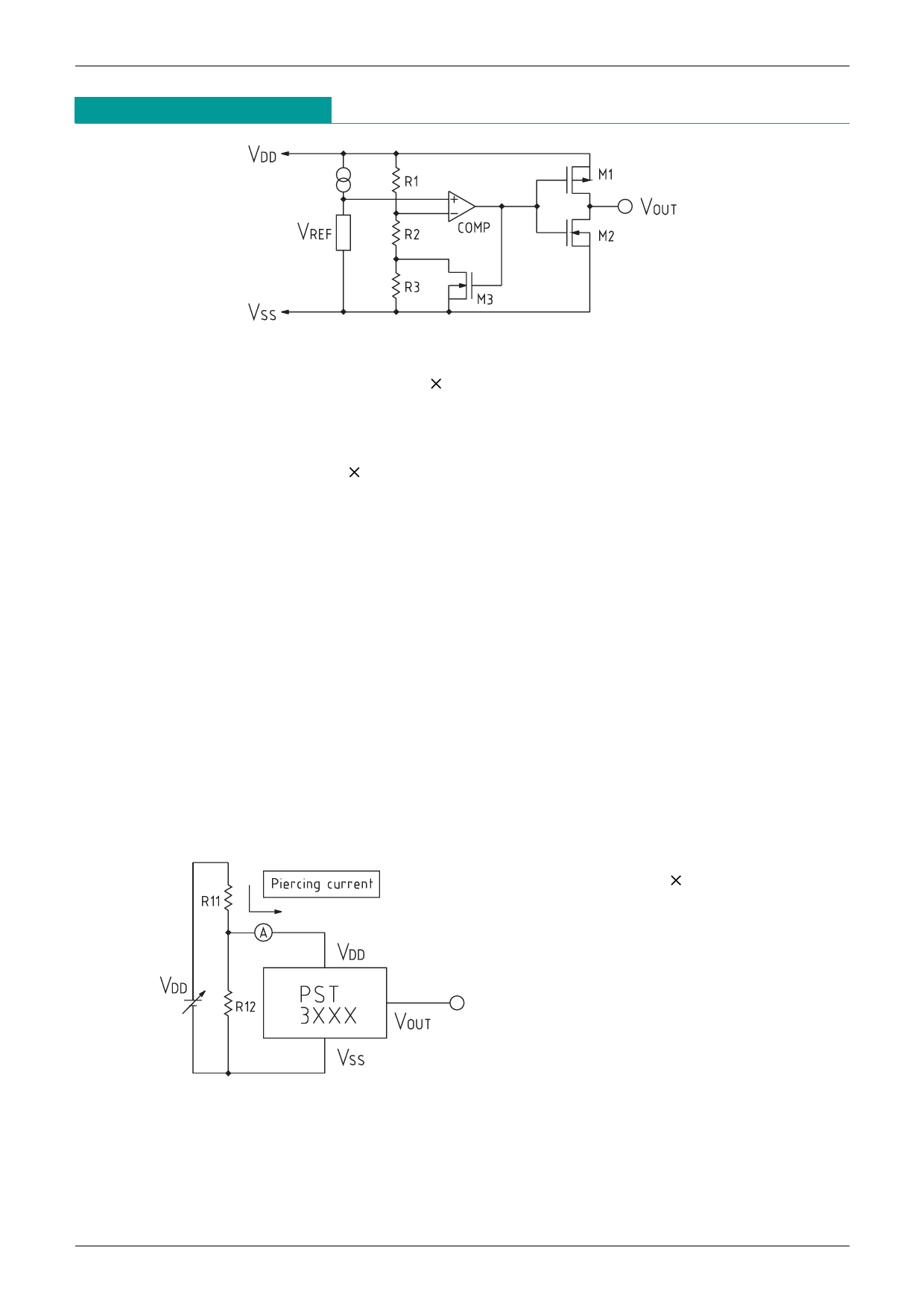
Description of Operation
IC for CMOS System Reset PST31XX~34XX
(1) VDD > VS, VOUT: H (M1: ON, M2, M3: OFF)
When VDD is gradually lowered from the above state, detection voltage is as follows.
Detection voltage: (R1 + R2 + R3) / (R2 + R3) VREF
(2) VDD < VS, VOUT: L (M1: OFF, M2, M3: ON)
When VDD is gradually raised from the above state, release voltage is as follows.
Release voltage = (R1 + R2) / (R2) VREF
(3) Hysteresis voltage = (release voltage) - (detection voltage).
(4) When VDD drops and goes below the minimum operating voltage, output is undefined; when output is
pulled up, output becomes VDD.
(5) VREF and detection resistors
1) The reference voltage source (VREF) for this IC is 0.8V typ. This gives excellent low power consumption
and temperature characteristics.
2) The high resistance process is used for resistors R1, R2 and R3 to achieve low consumption current for
the IC.
(6) Through current flows momentarily for detection and release. When using high VDD pin impedance, the
through current may cause oscillation.
(Example) Detection voltage changed by external settings
* The IC input voltage fluctuates due to the
through current R11 voltage drop, and
an oscillation state where detection and
release are repeated may occur.
* With CMOS output types, do not use as
shown in the diagram at left.
Share Link: 