74LV4094D Ver la hoja de datos (PDF) - Philips Electronics
Número de pieza
componentes Descripción
Fabricante
74LV4094D Datasheet PDF : 14 Pages
| |||
Philips Semiconductors
8-stage shift-and-store bus register
Product specification
74LV4094
FEATURES
• Optimized for low voltage applications: 1.0 to 3.6 V
• Accepts TTL input levels between VCC = 2.7 V and VCC = 3.6 V
• Typical VOLP (output ground bounce) < 0.8 V at VCC = 3.3 V,
Tamb = 25°C
• Typical VOHV (output VOH undershoot) > 2 V at VCC = 3.3 V,
Tamb = 25°C
• Output capability: standard
• ICC category: MSI
Applications:
• Serial-to-parallel data conversion
• Remote control holding register
DESCRIPTION
The 74LV4094 is a low-voltage Si-gate CMOS device and is pin and
function compatible with 74HC/HCT4094.
The 74LV4094 is an 8-stage serial shift register having a storage
latch associated with each stage for strobing data from the serial
input (D) to the parallel buffered 3-State outputs (QP0 to OP7). The
parallel outputs may be connected directly to the common bus lines.
Data is shifted on the positive-going clock (CP) transitions. The data
in each shift register is transferred to the storage register when the
strobe input (STR) is HIGH. Data in the storage register appears at
the outputs whenever the output enable input (OE) signal is HIGH.
Two serial outputs (QS1 and QS2) are available for cascading a
number of 74LV4094 devices. Data is available at QS1 on the
positive-going clock edges to allow high-speed operation in
cascaded systems in which the clock rise time is fast. The same
serial information is available at QS2 on the next negative going
clock edge and is for cascading 74LV4094 devices when the clock
rise time is slow.
QUICK REFERENCE DATA
GND = 0 V; Tamb = 25°C; tr =tf ≤ 2.5 ns
SYMBOL
PARAMETER
CONDITIONS
tPHL/tPLH
Propagation delay
CP to QS1
CP to QS2
CP to QPn
STR to QPn
CL = 15 pF;
VCC = 3.3 V
fMAX
Maximum clock frequency
CI
Input capacitance
CPD
Power dissipation capacitance per gate
VCC = 3.3 V
VI = GND to VCCNO TAG
NOTE:
1. CPD is used to determine the dynamic power dissipation (PD in µW)
PD = CPD × VCC2 × fi )ȍ (CL × VCC2 × fo) where:
fi = input frequency in MHz; CL = output load capacity in pF;
fo = output frequency in MHz; VCC = supply voltage in V;
ȍ (CL × VCC2 × fo) = sum of the outputs.
TYPICAL
14
13
18
17
95
3.5
83
UNIT
ns
MHz
pF
pF
ORDERING INFORMATION
PACKAGES
16-Pin Plastic DIL
16-Pin Plastic SO
TEMPERATURE RANGE OUTSIDE NORTH AMERICA
–40°C to +125°C
74LV4094 N
–40°C to +125°C
74LV4094 D
NORTH AMERICA
74LV4094 N
74LV4094 D
PKG. DWG. #
SOT38-4
SOT109-1
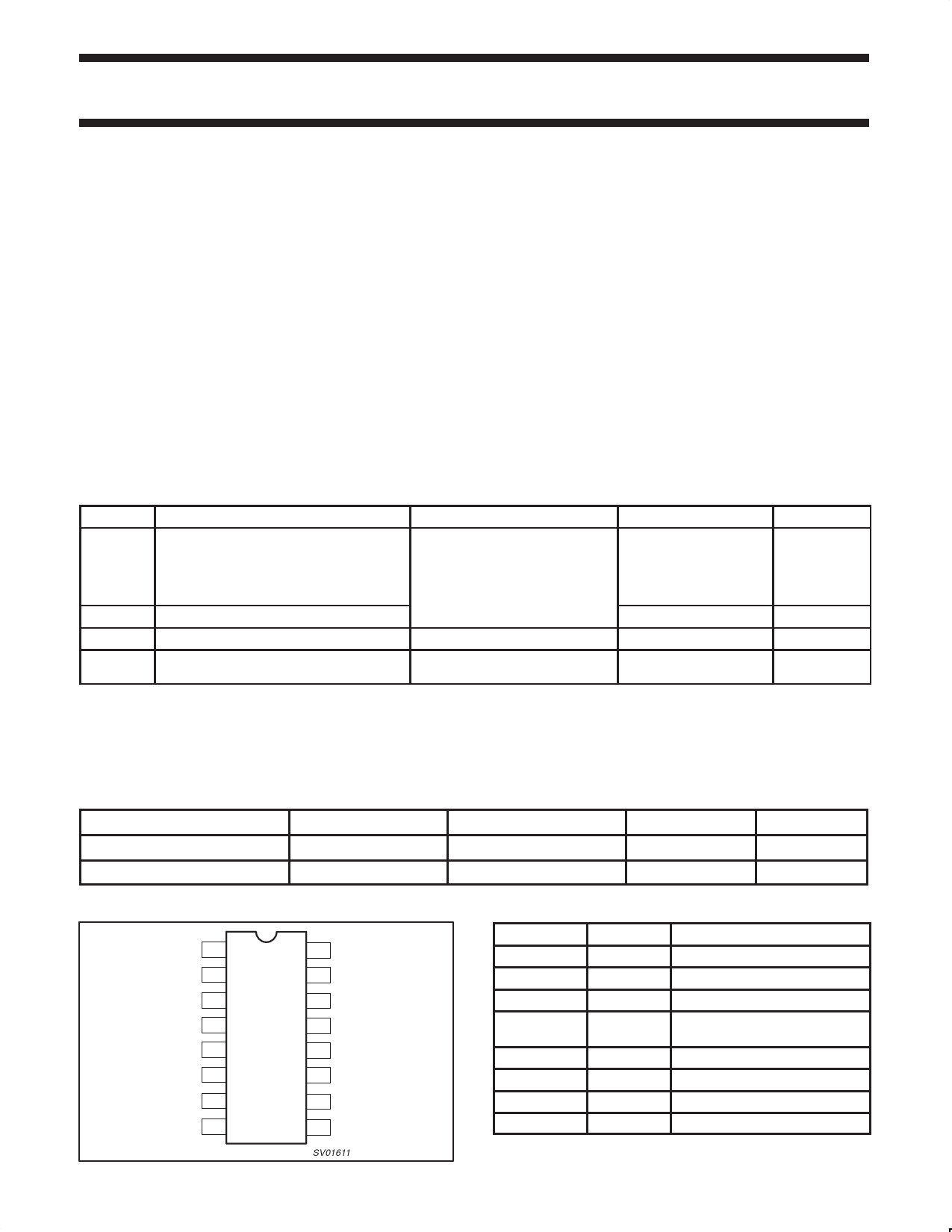
PIN CONFIGURATION
STR 1
D2
CP 3
QP0 4
QP1 5
QP2 6
QP3 7
GND 8
16 VCC
15 OE
14 QP4
13 QP5
12 QP6
11 QP7
10 QS2
9 QS1
SV01611
PIN DESCRIPTION
PIN NUMBER SYMBOL
1
STR
2
D
3
CP
4, 5, 6, 7, 14,
13, 12, 11
QP0 to QP7
8
GND
9, 10
15
QS1, QS2
OE
16
VCC
FUNCTION
Strobe input
Serial input
Clock input
Parallel outputs
Ground (0 V)
Serial outputs
Output enable input
Positive supply voltage
1998 Jun 23
2
853-2078 19619
Share Link: 