PM25LV010 Ver la hoja de datos (PDF) - PMC-Sierra
Número de pieza
componentes Descripción
Fabricante
PM25LV010 Datasheet PDF : 24 Pages
| |||
PMC
Pm25LV512/010
SERIAL INTERFACE DESCRIPTION
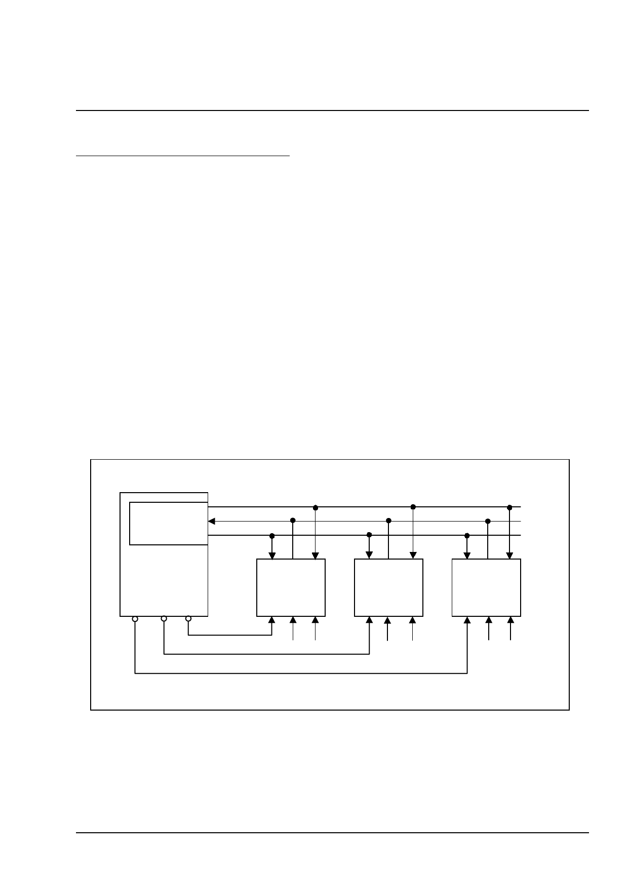
Pm25LV512/010 can be driven by a microcontroller on the SPI bus as shown in Figure 1. The serial communication
term definitions are in the following section.
MASTER: The device that generates the serial clock.
SLAVE: Because the Serial Clock pin (SCK) is always an input, the Pm25LV512/010 always operates as a slave.
TRANSMITTER/RECEIVER: The Pm25LV512/010 has separate pins designated for data transmission (SO) and
reception (Sl).
MSB: The Most Significant Bit (MSB) is the first bit transmitted and received.
SERIAL OP-CODE: After the device is selected with CE# going low, the first byte will be received. This byte
contains the op-code that defines the operations to be performed.
INVALID OP-CODE: If an invalid op-code is received, no data will be shifted into the Pm25LV512/010, and the serial
output pin (SO) will remain in a high impedance state until the falling edge of CE# is detected again. This will
reinitialize the serial communication.
Figure 1. Bus Master and SPI Memory Devices
SPI Interface with
(0, 0) or (1, 1)
Bus Master
CS3 CS2 CS1
SDO
SDI
SCK
SCK SO SI
SPI Memory
Device
SCK SO SI
SPI Memory
Device
SCK SO SI
SPI Memory
Device
CE#
WP# HOLD# CE#
WP# HOLD# CE#
WP# HOLD#
Note: 1. The Write Protect (WP#) and Hold (HOLD#) signals should be driven, High or Low as appropriate.
Programmable Microelectronics Corp.
5
Issue Date: December, 2003, Rev: 1.3
Share Link: 