PLL102-109XM Ver la hoja de datos (PDF) - PhaseLink Corporation
Número de pieza
componentes Descripción
Fabricante
PLL102-109XM Datasheet PDF : 10 Pages
| |||
Preliminary PLL102-109
Programmable DDR Zero Delay Clock Driver
ELECTRICAL SPECIFICATIONS
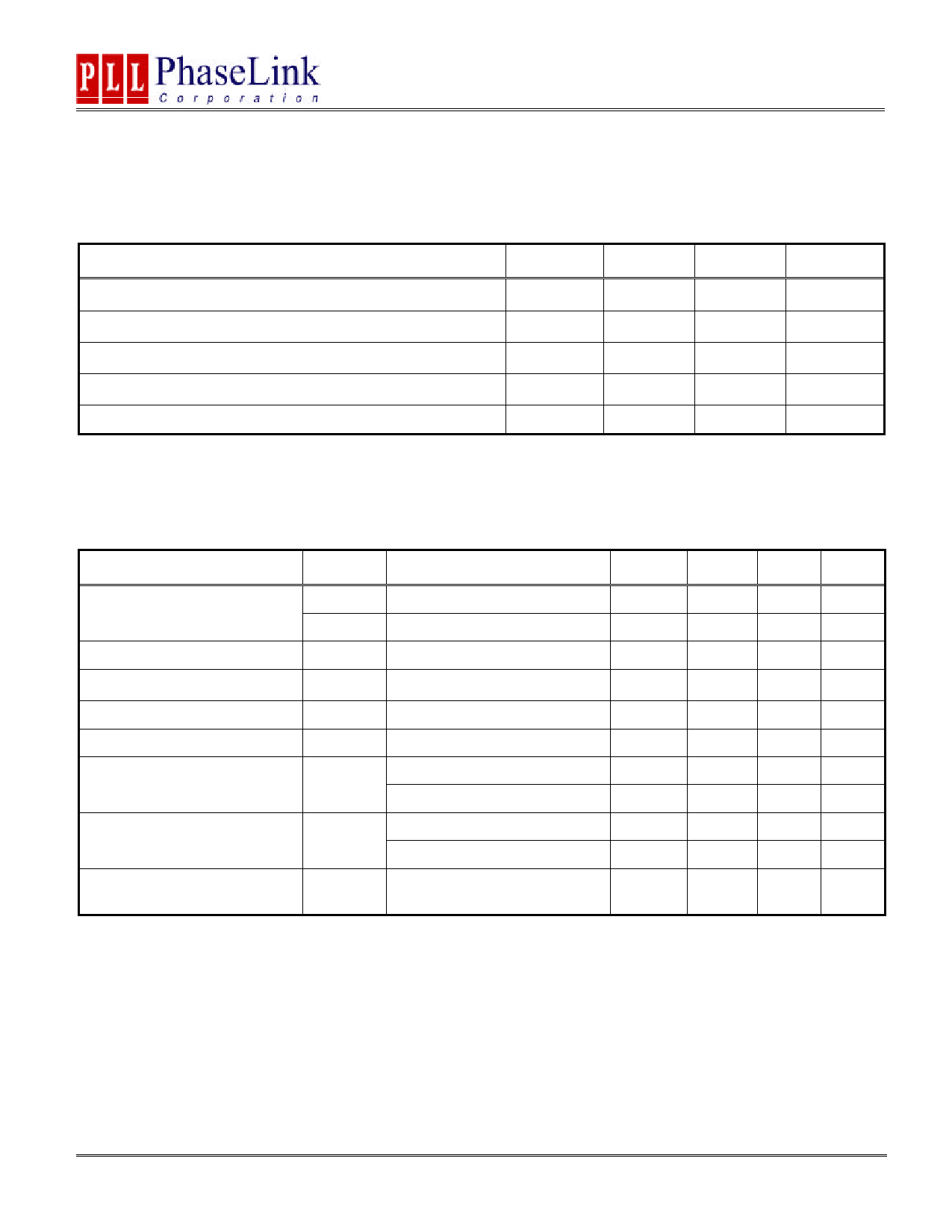
1. Absolute Maximum Ratings
PARAMETERS
SYMBOL
MIN.
MAX.
UNITS
Supply Voltage Range
Input Voltage Range
Output Voltage Range
Storage Temperature
Maximum power dissipation at TA = 550C in still air
VCC
-0.5
3.6
V
VI
-0.5
VCC+0.5
V
VO
-0.5
VCC+0.5
V
TS
-65
150
°C
PW
0.7
W
Exposure of the device under conditions beyond the limits specified by Maximum Ratings for extended periods may cause permanent damage to the
device and affect product reliability. These conditions represent a stress rating only, and functional operations of the device at these or any other con-
ditions above the operational limits noted in this specification is not implied.
2. Electrical Characteristics
PARAMETERS
Operating supply current
High Impedance output current
Input clamp voltage
Input Capacitance
Output Capacitance
High level output voltage
Low level output voltage
Output differential-pair crossing
voltage
SYMBOL
IDD2.5
IDDPD
IOZ
VIK
CIN
COUT
VOH
VOL
VOC
CONDITIONS
CL = 0 pF (Fclk=100Mhz)
CL = 0 pF
VDD=2.7V, VOUT=VDD or GND
Iin = -18mA
VI = VDD or GND
VO = VDD or GND
VDD = Min to Max, IOH = -1mA
VDD = 2.3V, IOH = -12mA
VDD = Min to Max, IOL = 1mA
VDD = 2.3V, IOL = 12mA
MIN.
VDD-0.1
1.7
(VDD/2)-
0.2
TYP.
250
2
3
MAX.
100
±10
-1.2
0.1
0.6
(VDD/
2)+0.2
UNITS
mA
uA
uA
V
pF
pF
V
V
V
V
V
47745 Fremont Blvd., Fremont, California 94538 TEL (510) 492-0990 FAX (510) 492-0991
Rev 02/26/03 Page 8
Share Link: 