PLL102-109XM Ver la hoja de datos (PDF) - PhaseLink Corporation
Número de pieza
componentes Descripción
Fabricante
PLL102-109XM Datasheet PDF : 10 Pages
| |||
Preliminary PLL102-109
Programmable DDR Zero Delay Clock Driver
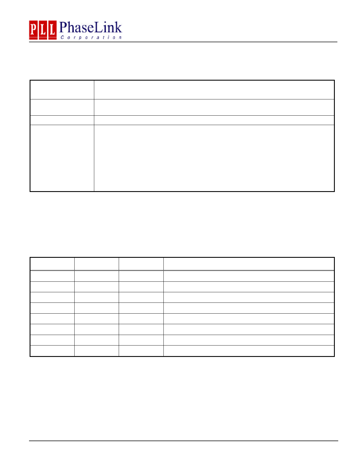
I2C BUS CONFIGURATION SETTING
Address Assignment
Slave Re-
ceiver/Transmitter
Data Transfer Rate
Data Protocol
A6
A5
A4
A3
A2
A1
A0
R/W
1
1
0
1
0
0
1
_
Provides both slave write and read back functionality
Standard mode at 100kbits/s
This serial protocol is designed to allow both blocks write and read from the controller. The
bytes must be accessed in sequential order from lowest to highest byte. Each byte transferred
must be followed by 1 acknowledge bit. A byte transferred without acknowledged bit will termi-
nate the transfer. The write or read block both begins with the master sending a slave address
and a write condition (0xD4) or a read condition (0xD5).
Following the acknowledge of this address byte, in Write Mode: the Command Byte and Byte
Count Byte must be sent by the master but ignored by the slave, in Read Mode: the Byte
Count Byte will be read by the master then all other Data Byte. Byte Count Byte default at
power-up is = (0x09).
I2C CONTROL REGISTERS
1. BYTES 0 TO 4 are reserved power up default =1.
2. BYTE 5: Outputs Register (1=Enable, 0=Disable)
Bit
Pin#
Default Description
Bit 7
-
-
Reserved
Bit 6
-
-
Reserved
Bit 5
26,27
1
CLKT5, CLKC5 (1= active, 0=inactive)
Bit 4
24,25
1
CLKT4, CLKC4 (1= active, 0=inactive)
Bit 3
16,17
1
CLKT3, CLKC3 (1= active, 0=inactive)
Bit 2
13,14
1
CLKT2, CLKC2 (1= active, 0=inactive)
Bit 1
4,5
1
CLKT1, CLKC1 (1= active, 0=inactive)
Bit 0
1,2
1
CLKT0, CLKC0 (1= active, 0=inactive)
47745 Fremont Blvd., Fremont, California 94538 TEL (510) 492-0990 FAX (510) 492-0991
Rev 02/26/03 Page 3
Share Link: 