PI90LV018A Ver la hoja de datos (PDF) - Pericom Semiconductor
Número de pieza
componentes Descripción
Fabricante
PI90LV018A Datasheet PDF : 9 Pages
| |||
PI90LV032A/PI90LV028A/PI90LV018A
1122334455667788990011223344556677889900112233445566778899001122112233445566778899001122334455667788990011223344556677889900112211223344556677889900311V223344L5566V778899D0011S2233H445566i77g88h9900-11S2211p22e3344e55d667788D9900i11f22f33e44r5566e77n8899t00i11a22l3344L5566i77n8899e0011R2211e22c3344e55i66v7788e99r00s1122
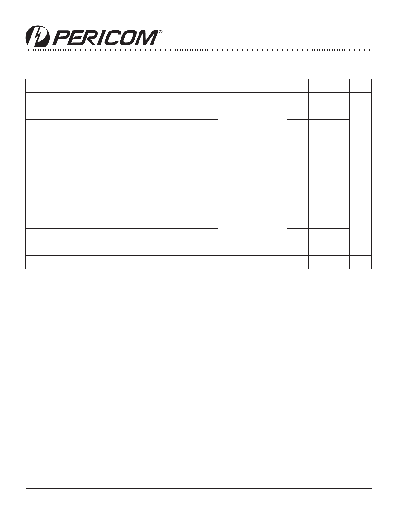
Switching Characteristics
Over supply voltage and operating temperature ranges, unless otherwise specified. (Notes 3,4,7,8)
Symbol
Parameter
Conditions
Min. Typ. Max. Units
tPHLD
tPLHD
tSKD1
tSKD2
tSKD3
tSKD4
tTLH
tTHL
tPHZ
tPLZ
tPZH
tPZL
tMAX
Differential Propagation Delay High to Low (VCM = 1.2V)
Differential Propagation Delay Low to High (VCM = 1.2V)
Differential Pulse Skew | tPHLD - tPLHD |(6)
Differential Channel-to-Channel Skew-same device(7)
Differential Part-to-Part Skew(8)
Differential Part-to-Part Skew(9)
Rise Time
Fall Time
Disable Time High to Z
Disable Time Low to Z
Enable Time Z to High
Enable Time Z to Low
Maximum Operating Frequency(13)
CL = 10pF
VID = 200mV
(Figures 1 & 2)
RL = 2KΩ
CL = 10pF
(Figures 3 & 4)
All channels switching
1.8
4.7
1.8
4.7
0 0.1 0.35
0 0.1 0.5
1.0
1.5
ns
0.35 1.2
0.35 1.2
8 12
6 12
11 17
11 17
200 250
MHz
Notes:
1. “Absolute Maximum Ratings” are those values beyond which the safety of the device cannot be guaranteed. They are not meant to imply
that the devices should be operated at these limits. The table of “Electrical Characteristics” specifies conditions of device operation.
2. Current into device pins is defined as positive. Current out of device pins is defined as negative. All voltages are referenced to ground unless
otherwise specified.
3. All typicals are given for: VCC = +3.3V, TA = +25°C.
4. Generator waveform for all tests unless otherwise specified: f = 1 MHz, ZO = 50Ω, tR and tF (0% to 100%) ≤ 3ns for RIN.
5. The VCMR range is reduced for larger VID. Example : if VID = 400mV, the VCMR is 0.2V to 2.2V. The fail-safe condition with inputs
shorted is valid over a common-mode range of 0V to 2.3V. A VID up tp VCC - 0V may be applied to the RIN+ / RIN- inputs with the
Common-Mode voltage set to VCC/2. Propagation delay and Differential Pulse skew decrease when VID is increased from 200mV to
400mV. Skew specifications apply for 200mV ≤ VID ≤ 800mV over the common mode range.
6. tskd1 is the magnitude difference in differential propagation delay time between the positive going edge and the negative going edge of the
same channel.
7. tSKD2, Channel-to-Channel Skew, is defined as the difference between the propagation delay of one channel and that of the others on the
same chip with any event on the inputs.
8. tSKD3, Part-to-Part Skew, is the differential Channel-to-Channel skew of any event between devices. This specification applies to devices
at the same VCC,and within 5ºC of each other within the operating temperature range.
9. tSKD4, Part-to-Part Skew, is the differential Channel-to-Channel skew of any event between devices. This specification applies
to devices over recommended operating temperature and voltage ranges, and across process distribution. tskd4 is defined as IMax - Mini
differential propagation delay.
10. Output short circuit current (IOS) is specified as magnitude only, minus sign indicates direction only. Only one output should be shorted at
a time, do not exceed maximum junction temperature specification.
11. CL includes probe and jig capacitance.
12. VCC is always higher than RIN+ and RIN- voltage. RIN- and RIN+ are allowed to have a voltage range -0.2V to VCC- VID/2.
However, to be compliant with AC specifications, the common voltage range 0.1V to 2.3V.
13. fmax generator input conditions: tR = tF < 1ns, (0% to 100%), 50% duty cycle, differential (1.05V to1.35V peak to peak).
Output Criteria: duty cycle = 60%/40%, VOL (max 0.4V), VOH (min 2.7V), Load = 10pF (stray plus probes).
08-0295
4
PS8423D
11/11/08
Share Link: 