PI6C2405A(2010) Ver la hoja de datos (PDF) - Pericom Semiconductor
Número de pieza
componentes Descripción
Fabricante
PI6C2405A Datasheet PDF : 8 Pages
| |||
PI6C2405A
Zero Delay Clock Buffer
Zero Delay and Skew Control
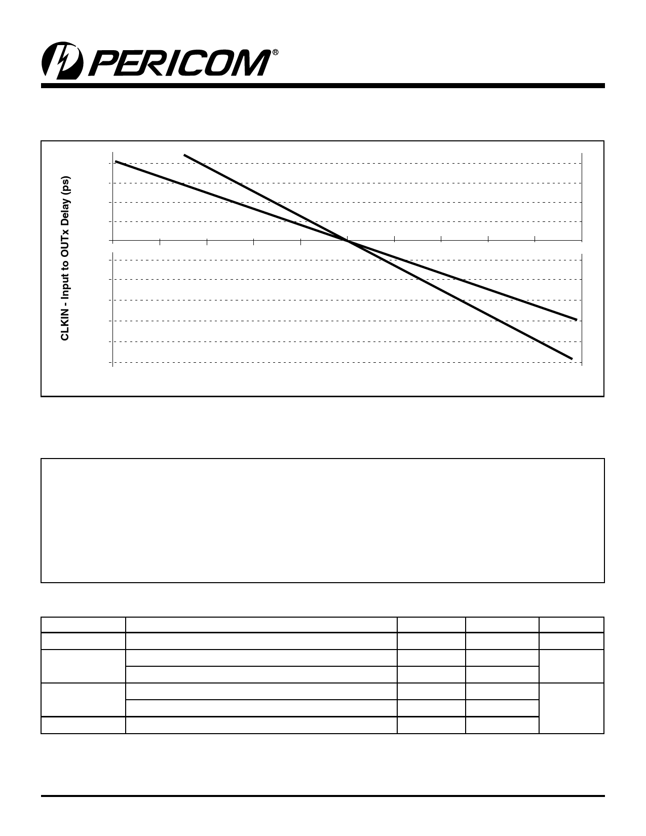
CLKIN Input to OUTx Delay vs. Difference in Loading between OUT0 pin and OUTx pins
800
600
400
200
0
-25
-20
-15
-10
-5
0
5
10
15
20
25
-200
-400
-600
PI6C2405A-1H
-800
-900
PI6C2405A-1
-1000
Output Load Difference: OUT0 Load - OUTx Load (pF)
The relationship between loading of the OUT0 signal and other outputs determines the input-output delay. Zero delay is achieved when
all outputs, including feedback, are loaded equally.
Maximum Ratings
Supply Voltage to Ground Potential............................................................................................................................. –0.5V to +7.0V
DC Input Voltage (Except CLKIN)......................................................................................................................–0.5V to VDD +0.5V
DC Input Voltage CLKIN..................................................................................................................................................... –0.5 to 7V
Storage Temperature................................................................................................................................................... –65ºC to +150ºC
Maximum Soldering Temperature (10 seconds).......................................................................................................................... 260ºC
Junction Temperature................................................................................................................................................................... 150ºC
Static Discharge Voltage (per MIL-STD-883, Method 3015).................................................................................................. >2000V
Operating Conditions (VCC = 3.3V ±0.3V)
Parameter
Description
VDD
Supply Voltage
Commerical Operating Temperature
TA
Industrial Operating Temperature
Load Capacitance, below 100 MHz
CL
Load Capacitance, from 100 MHz to 133
CIN
Input Capacitance
Min.
3.0
0
-40
Max.
3.6
70
85
30
15
7
Units
V
°C
pF
11-0001
2
PS8592I
04/29/10
Share Link: 