PI6C10804 Ver la hoja de datos (PDF) - Pericom Semiconductor
Número de pieza
componentes Descripción
Fabricante
PI6C10804 Datasheet PDF : 7 Pages
| |||
PI6C10804
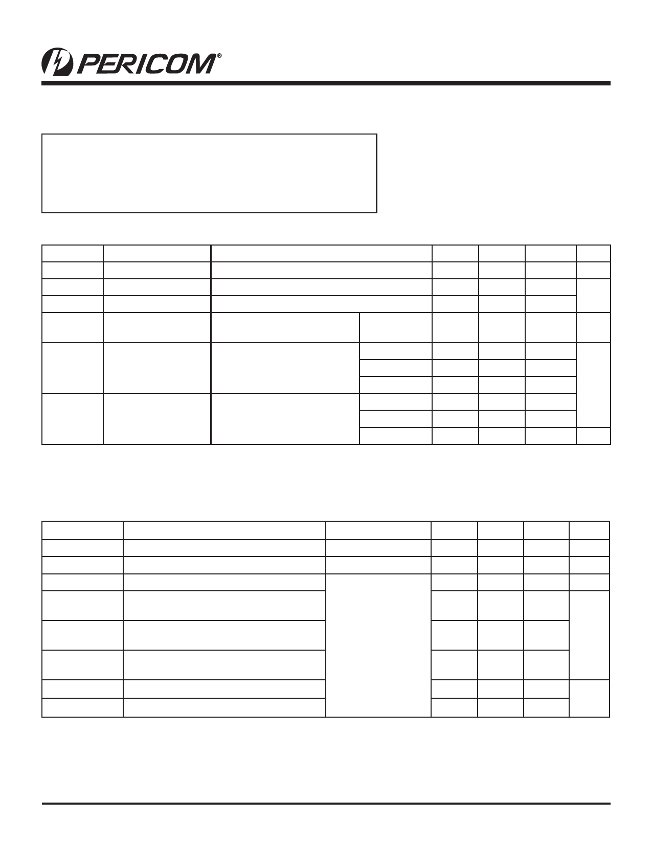
1.5V/1.8V/2.5V, 180MHz, 1:4 Networking Clock Buffer
2.5V Absolute Maximum Ratings (Above which the useful life may be impaired. For user guidelines only, not tested.)
Note:
Storage Temperature........................................................... –65°C to +150°C Stresses greater than those listed under MAXIMUM
VDD Voltage ..........................................................................–0.5V to +3.6V
Output Voltage............................................................... –0.5V to VDD+0.5V
RATINGS may cause permanent damage to the
device. This is a stress rating only and functional operation
of the device at these or any other conditions above those
Input Voltage .......................................................................................... 3.6V indicated in the operational sections of this specification is
not implied. Exposure to absolute maximum rating condi-
tions for extended periods may affect reliability.
2.5V DC Characteristics (Over Operating Range: VDD = 2.5V ± 0.2V, TA = -40° to 85°C)
Parameters Description
Test Conditions(1)
Min.
VDD
Supply Voltage
2.3
VIH
Input HIGH Voltage Logic HIGH level
1.7
VIL
Input LOW Voltage Logic LOW level
-0.3
II
Input Current
VDD = Max, VIN = VDD or
GND
I pin
IOH = -1mA 2.0
VOH
Output High Voltage VDD = Min., VIN = VIH or VIL IOH = -2mA 1.7
IOH = -8mA 1.5
IOL = 1mA
VOL
Output LOW Voltage VDD = Min., VIN - VIH or VIL IOL = 2mA
Notes:
1. For Max. or Min. conditions, use appropriate operating range values.
2. Typical values are at VDD = 2.5V, +25°C ambient and maximum loading.
IOL = 8mA
Typ. (2)
2.5
Max.
2.7
3.6
0.7
15
0.4
0.7
0.7
Units
V
V
μA
V
V
2.5V AC Characteristics (Over Operating Range: VDD = 2.5V ± 0.2V, TA = -40° to 85°C)
Parameters
Description
Test Conditions(1) Min. Typ
FIN
tR/tF
tPLH, tPHL(2)
tSK(O)(3)
Input Frequency
CLKn Rise/Fall Time
20% to 80%
Propagation Delay BUF_IN to CLKn
Output to Output Skew between any two
outputs of the same device @ same transition
0
1.0
1.5
tSK(P)(3)
Pulse Skew between opposite transitions
(tPHL-tPLH) of the same output
CL = 5pF, 125 MHz
Outputs are measured
100
tSK(T)(3)
Part to Part Skew between two identical out- @ VDD/2
puts of different parts on the same board(4)
tdc_in
Duty Cycle In @ 1ns edge rate
45
tdc_out
Duty Cycle Out
40
Notes:
1. See test circuit and waveforms.
2. Minimum limits are guaranteed but not tested on Propagation Delays.
3. Skew measured at worse cast temperature (max. temp).
4. Identical conditions: loading, transitions, supply voltage, temperature, package type and speed grade.
Max.
250
1
2.0
70
Units
MHz
ns
ns
200
ps
300
55
%
60
09-0056
2
PS8822G 10/07/09
Share Link: 