HT48RA3(2007) Ver la hoja de datos (PDF) - Holtek Semiconductor
Número de pieza
componentes Descripción
Fabricante
HT48RA3 Datasheet PDF : 38 Pages
| |||
HT48RA3/HT48CA3
will be serviced. This feature prevents stack overflow al-
lowing the programmer to use the structure more easily.
In a similar case, if the stack is full and a ²CALL² is sub-
sequently executed, stack overflow occurs and the first
entry will be lost (only the most recent 8 return ad-
dresses are stored).
Data Memory - RAM
The data memory is designed with 250´8 bits. The
data memory is divided into two functional groups: spe-
cial function registers and general purpose data mem-
ory (224´8). Most are read/write, but some are read
only.
The special function registers include the indirect ad-
dressing registers (R0;00H, R1;02H) bank pointer (BP;
04H), Timer/Event Counter 0 (TMR0;0DH),
Timer/Event Counter 0 control register (TMR0C;0EH),
Timer/Event Counter 1 higher order byte register
(TMR1H;0FH), Timer/Event Counter 1 lower order byte
register (TMR1L;10H), Timer/Event Counter 1 control
register (TMR1C;11H), program counter lower-order
byte register (PCL;06H), memory pointer registers
(MP0;01H, MP1;03H), accumulator (ACC;05H), table
pointer (TBLP;07H, TBHP;1FH), table higher-order
byte register (TBLH;08H), status register (STATUS;
0AH), interrupt control register (INTC;0BH), Watchdog
Timer option setting register (WDTS;09H), I/O regis-
ters (PA;12H, PB;14H, PC;16H, PF;1CH), and I/O con-
trol registers (PAC;13H, PBC;15H, PCC;17H,
PFC;1DH). The remaining space before the 20H is re-
served for future expanded usage and reading these
locations will get ²00H². The general purpose data
memory, addressed from 20H to FFH, is used for data
and control information under instruction commands.
All of the data memory areas can handle arithmetic,
logic, increment, decrement and rotate operations di-
rectly. Except for some dedicated bits, each bit in the
data memory can be set and reset by ²SET [m].i² and
²CLR [m].i². They are also indirectly accessible through
memory pointer registers (MP0 or MP1).
Indirect Addressing Register
Location 00H and 02H are indirect addressing registers
that are not physically implemented. Any read/write op-
eration of [00H] ([02H]) will access data memory pointed
to by MP0 (MP1). Reading location 00H (02H) itself indi-
rectly will return the result 00H. Writing indirectly results
in no operation.
The memory pointer registers (MP0 and MP1) are 8-bit
registers.
Accumulator
The accumulator is closely related to ALU operations. It
is also mapped to location of the data memory and can
carry out immediate data operations. The data move-
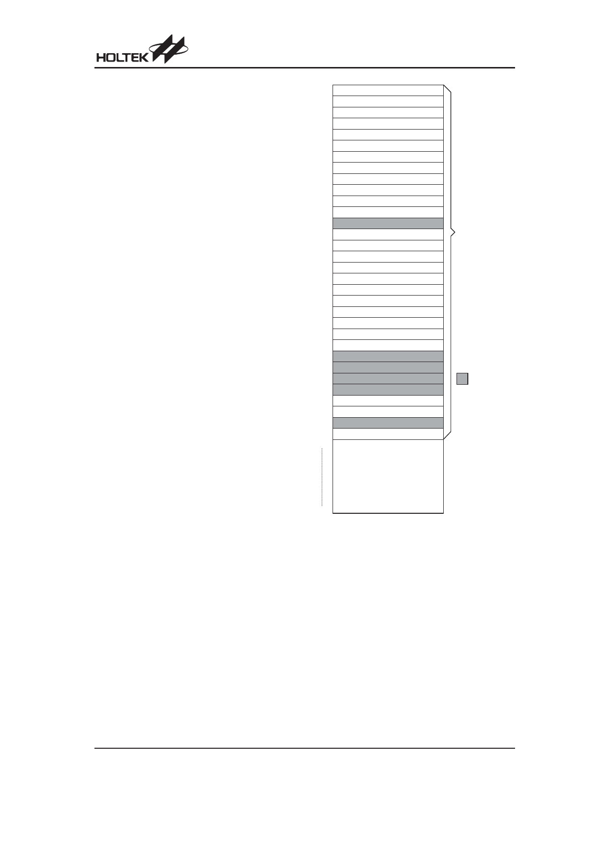
00H
In d ir e c t A d d r e s s in g R e g is te r 0
01H
M P0
02H
In d ir e c t A d d r e s s in g R e g is te r 1
03H
M P1
04H
BP
05H
ACC
06H
PCL
07H
TB LP
08H
TB LH
09H
W D TS
0A H
STATU S
0B H
IN T C
0C H
0D H
TM R 0
0E H
TM R 0C
0FH
TM R 1H
10H
TM R 1L
11H
TM R 1C
12H
PA
13H
PAC
14H
PB
15H
PBC
16H
PC
17H
PCC
18H
19H
1A H
1B H
1C H
PF
1D H
PFC
1E H
1FH
TBH P
20H
G e n e ra l P u rp o s e
D ATA M EM O R Y
(2 2 4 B y te s )
S p e c ia l P u r p o s e
D ATA M EM O R Y
:U nused
R e a d a s "0 0 "
FFH
RAM Mapping
ment between two data memory locations must pass
through the accumulator.
Arithmetic and Logic Unit - ALU
This circuit performs 8-bit arithmetic and logic opera-
tions. The ALU provides the following functions:
· Arithmetic operations (ADD, ADC, SUB, SBC, DAA)
· Logic operations (AND, OR, XOR, CPL)
· Increment and decrement (INC, DEC)
· Rotation (RL, RR, RLC, RRC)
· Increment and Decrement (INC, DEC)
· Branch decision (SZ, SNZ, SIZ, SDZ ....)
The ALU not only saves the results of a data operation
but also changes the status register.
Rev. 1.30
8
October 12, 2007
Share Link: 