PDSP16340 Ver la hoja de datos (PDF) - Zarlink Semiconductor Inc
Número de pieza
componentes Descripción
Fabricante
PDSP16340 Datasheet PDF : 14 Pages
| |||
PDSP16340
ABSOLUTE MAXIMUM RATINGS (Note 1)
Supply voltage Vcc
-0.5V to 7.0V
Input voltage V
-0.5V to Vcc + 0.5V
IN
Output voltage VOUT
-0.5V to Vcc + 0.5V
Clamp diode current per pin I (see note 2)
18mA
K
Static discharge voltage (HMB)
500V
Storage temperature T
S
-65°C to 150°C
Ambient temperature with power applied T
AMB
Military
-55°C to +125°C
Industrial
-40°C to 85°C
Junction temperature
150°C
Package power dissipation
3500mW
Thermal resistances
Junction to Case Ø
JC
5°C/W
NOTES
1. Exceeding these ratings may cause permanent damage.
Functional operation under these conditions is not implied.
2. Maximum dissipation or 1 second should not be exceeded,
only one output to be tested at any one time.
3. Exposure to absolute maximum ratings for extended peri-
ods may affect device reliablity.
4. Vcc = Max. Outputs Unloaded, Clock Freq = Max.
5. CMOS levels are defined as
VIH = Vcc - 0.5v
V = +0.5v
IL
6. Current is defined as negative into the device.
7. Ø data assumes that heat is extracted from the top face of
JC
the package.
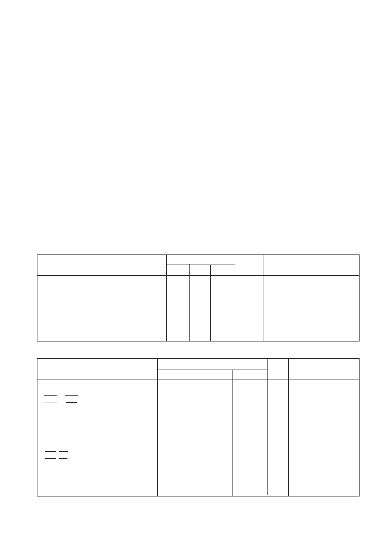
ELECTRICAL CHARACTERISTICS
Operating Conditions (unless otherwise stated)
Commercial: TAMB = -0°C to +70°C TJ(MAX) = 95°C VCC = 5.0V±5% Ground = 0V
Industrial:
T
AMB
=
-40°C
to
+85°C
T
J(MAX)
=
110°C
V
CC
=
5.0V±10%
Ground
=
0V
Military: TAMB = -55°C to +125°C TJ(MAX) = 150°C VCC = 5.0V±10% Ground = 0V
Static Characteristics
Characteristic
Symbol
Value
Min. Typ. Max.
Units Conditions
Output high voltage
Output low voltage
Input high voltage
Input low voltage
Input leakage current
Input capacitance
Output leakage current
Output S/C current
V
OH
2.4
-
V
I = 4mA
OH
VOL
-
0.4
V
IOL = -4mA
V
IH
3.0
-
V
VIL
-
0.8
V
I
IN
-10
+10
µA
GND < V < V
IN
CC
C
10
IN
pF
I
OZ
-50
+50
µA
GND < V < V
OUT
CC
I
SC
10
250
mA
VCC = Max
Switching Characteristics
Characteristic
M15:0 or P15:0 setup to clock rising edge
M15:0 or P15:0 hold after clock rising edge
MEN or PEN setup to clock rising edge
MEN or PEN hold after clock rising edge
RANGE setup to clock rising edge
RANGE hold after clock rising edge
Clock rising edge to all outputs valid
Clock freq
Clock High Time
Clock Low Time
OER,OEI low to data valid
OER,OEI high to data high impedance
Pipeline delay VIN to VOUT
Vcc Current (CMOS inputs)
Vcc Current (TTL inputs)
Industrial
Min.
15
4
20
0
15
8
5
DC
15
20
-
-
28
-
-
Typ.
Max.
-
-
-
-
-
-
30
20
-
-
20
20
28
430
460
Military
Units
Min.
15
4
20
0
15
8
5
DC
15
20
-
-
28
-
-
Typ.
Max.
- ns
- ns
- ns
- ns
- ns
- ns
30 ns
20 MHz
- ns
- ns
20 ns
20 ns
28 CLKs
450 mA
500 mA
Conditions
30pF
see Fig. 6
see Fig. 6
see Note 4
see Note 4
7
Share Link: 