PDSP16340 Ver la hoja de datos (PDF) - Zarlink Semiconductor Inc
Número de pieza
componentes Descripción
Fabricante
PDSP16340 Datasheet PDF : 14 Pages
| |||
PDSP16340
VIN
P15:0 PEN MODE
M15:0 MEN RANGE
DELAY
CORDIC PROCESSOR ARRAY
Magnitude Adjust
and
Saturate at SQRT(2)
UNITY
SELECT
DELAY
OER
VOUT
XR15:0
OEI
XI15:0
SAT
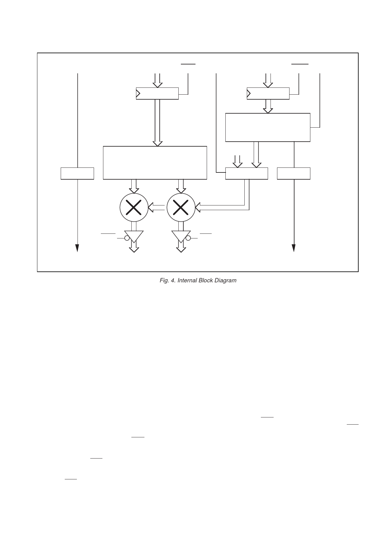
Fig. 4. Internal Block Diagram
OPERATION
The functional blocks used within the device are illus-
trated by Fig. 4. Both input data and output data are fully
registered to allow the device to be easily incorporated into
data flow DSP systems. The sine and cosine values are
actually calculated in a 26 stage pipelined arithmetic proces-
sor, and are accurate to 16 bits. This technique allows high
data throughputs, and requires less die area than the equiva-
lent ROM.
The PDSP16340 has two modes of operation, which are
selected by the logical state of the MODE input pin. This pin
should be tied high or low to suite the particular application.
Look-up Mode
In the Table Look-up mode the MODE pin is tied high, and
the device is used to provide simultaneous sine and cosine
values at rates up to the maximum clock frequency. A new
phase value is clocked into the Phase Port (P15:0) on each
cycle, and the corresponding sine and cosine values appear
at the XI and XR ports 29 clock cycles later. In this operating
mode the MAGNITUDE inputs, the MEN, and the RANGE
inputs are logically redundant. They must, however, be tied
either high or low for electrical reasons. If the Phase Port is
disabled by pulling PEN high, then the look-up table will
continue to provide the sine and cosine outputs corresponding
to the value of P15:0 present during the active clock edge
before the PEN level change.
Fig. 5. illustrates a typical FFT arrangement with the
PDSP16340 providing sine and cosine ‘twiddle’ factors for use
by the butterfly processor. Use of the PDSP16520 Quad Port
RAM, and the PDSP16116 / 318 complex arithmetic element,
allows butterfly calculations to be performed at rates up to
20 MHz.
Coordinate Conversion
In the Coordinate Conversion Processor mode the MODE
pin is tied low, and the PDSP16340 converts data from polar
format into the corresponding real and imaginary Cartesian
co-ordinates. The coordinate conversion operation is equiva-
lent to the inverse of the function performed by the
PDSP16330 Pythagoras Processor. The device produces
simultaneous sine and cosine values from the incoming phase
angle, and then multiplies these results with the appropriate
magnitude value. The MEN input allows the value in the input
latch to be retained in a similar manner to the use of the PEN
control.
The RANGE control allows the device to accept magni-
tude data in the range of, either, -1 to within one LSB of +1, or
from -2 to within one LSB of +2. The smaller range option
allows maximum accuracy to be preserved, if fractional inputs
are expected.The latter option enables the theoretical maxi-
mum polar magnitude of SQRT(2) to be accommodated. A
negative magnitude introduces a 180° phase shift.
5
Share Link: 