PDSP16340 Ver la hoja de datos (PDF) - Zarlink Semiconductor Inc
Número de pieza
componentes Descripción
Fabricante
PDSP16340 Datasheet PDF : 14 Pages
| |||
PDSP16340
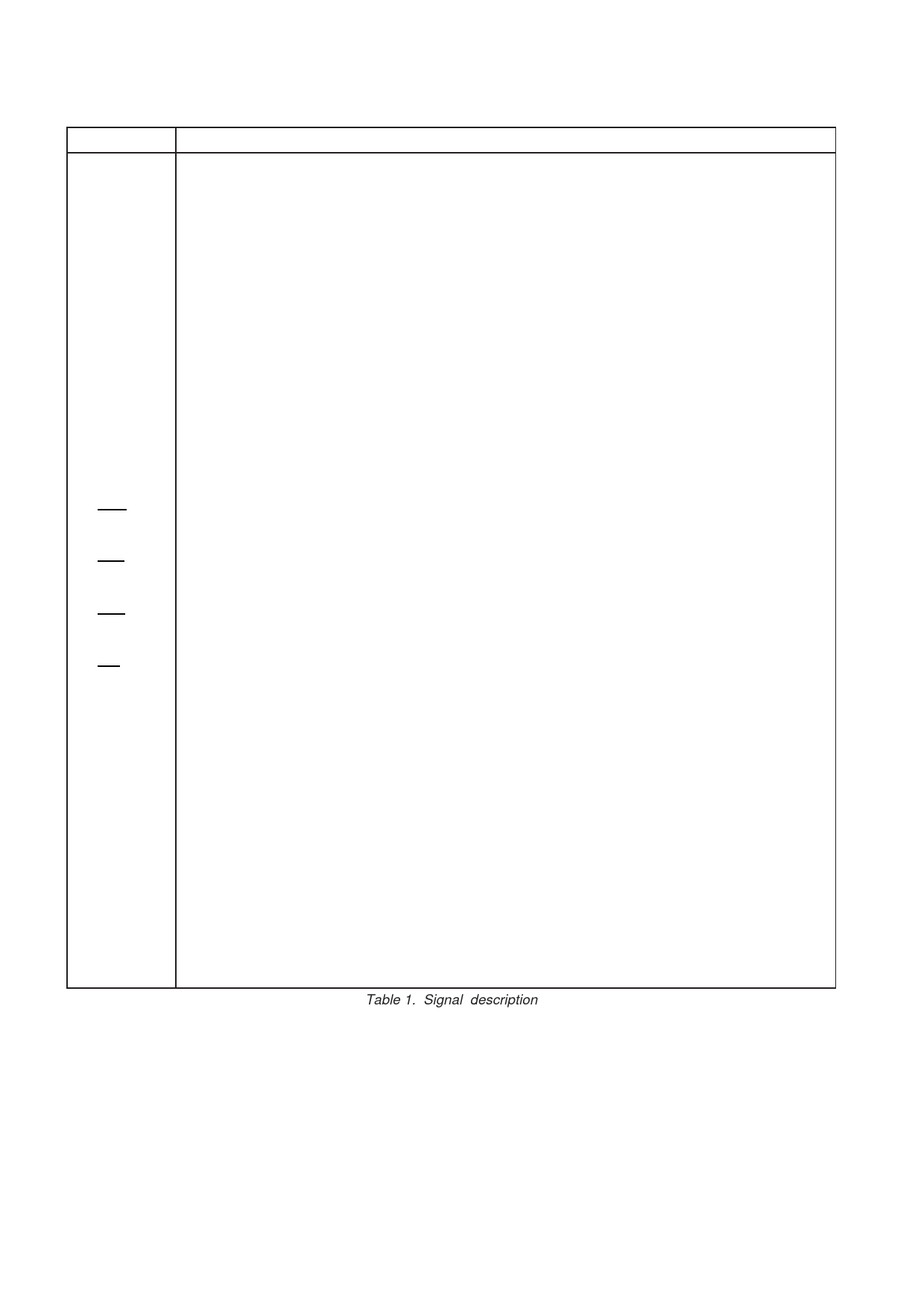
SIGNAL
M15:0
P15:0
XR15:0
XI15:0
RANGE
SAT
MEN
PEN
OER
OEI
VIN
VOUT
MODE
CLK
VDD
GND
DESCRIPTION
16 bit 2's complement data representing the magnitude of the phase angle. Data is loaded into the
input register on the rising edge of CLK. These inputs are not used in look-up table mode, however,
they should be tied high or low for electrical, rather than logical, reasons. M15 is the MSB.
16 bit data representing the phase angle. Data is loaded into the input register on the rising edge
of CLK. P15 is the MSB.
16 bit 2’s complement real data output, or cosine output in the table look-up mode. Data is passed
to the XR outputs on the rising edge of CLK.
16 bit 2’s complement imaginary data output, or sine output in the table look-up mode. Data is
passed to the XI outputs on the rising edge of CLK.
Magnitude range select. When this pin is high, the MSB of the M input bus (also the sign bit) will
represent 21. When low, it will represent 20
Input data saturated flag. This output goes high to indicate that input data of magnitude greater than
SQRT(2) has been saturated to SQRT(2). It is internally delayed such that it appears at the output
at the same time as the data which resulted from the saturated input value.
Clock enable for the magnitude input port. When low new data may be latched in the input register;
when high the register remains in its previous state.
Clock enable for the phase input port. When low new data may be latched in the input register: when
high the register remains in its previous state.
Output enable for the XR output port. When high the XR output is forced into a high impedance
state.
Output enable for the XI output port. When high the XI output is forced into a high impedance state.
Valid data input flag. This input is connected to VOUT via a pipeline delay which matches the data
path pipeline delay. Hence, if VIN is set high when valid data is input, then VOUT will go high when
valid results are output. It performs no internal control function.
Valid data output flag which is a delayed version of VIN as explained above.
When high, this input configures the chip into look-up table mode in which the M inputs are
redundant and internally replaced by a unity magnitude. When low, the chip is configured in
coordinate conversion mode.
Common clock to all internal registers.
Four +5V power pins. All power supply pins must be connected.
Four ground pins. All pins must be connected.
Table 1. Signal description
4
Share Link: 