PCK2002PD Ver la hoja de datos (PDF) - Philips Electronics
Número de pieza
componentes Descripción
Fabricante
PCK2002PD Datasheet PDF : 8 Pages
| |||
Philips Semiconductors
140 MHz PCI-X clock buffer
Product data
PCK2002P
AC CHARACTERISTICS
SYMBOL
PARAMETER
TEST CONDITIONS
NOTES
LIMITS
Tamb = –40 to +85 °C
MIN
TYP6
MAX
TH
CLK HIGH time
TL
CLK LOW time
2
6.0
—
—
66 MHz
3
6.0
—
—
TH
CLK HIGH time
TL
CLK LOW time
2
2.9
—
—
140 MHz
3
3.0
—
—
TR
Output rise slew rate
4
1.4
1.7
4.0
TF
Output fall slew rate
4
1.5
2.2
4.0
TPLH
Buffer LH propagation delay
5
1.8
2.9
3.4
TPHL
Buffer HL propagation delay
5
1.8
2.8
3.4
TSKW
Bus CLK skew
1
—
—
200
TDDSKW
Device to device skew
1
—
—
500
NOTES:
1. CLK skew is only valid for equal loading of all outputs.
2. TH is measured at 0.5 VDD as shown in Figure 2.
3. TL is measured at 0.35 VDD as shown in Figure 2.
4. TR and TF are measured as a transition through the threshold region 0.2 VDD to 0.6 VDD and 0.6 VDD to 0.2 VDD.
5. Input edge rate for these tests must be faster than 1 V/ns.
6. All typical values are at VCC = 3.3 V and Tamb = 25 °C.
UNIT
ns
ns
ns
ns
V/ns
V/ns
ns
ns
ps
ps
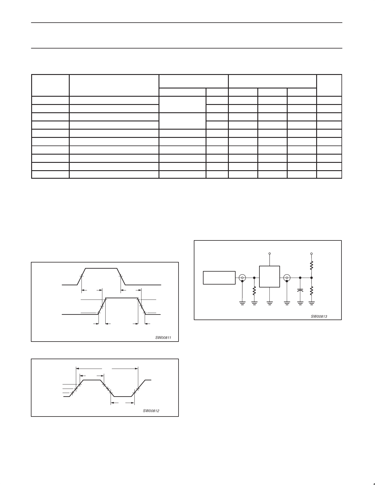
AC WAVEFORMS
VM = 50% VDD
CL = 25 pF
VOL and VOH are the typical output voltage drop that occur with the
output load.
BUF_IN
INPUT
VDD
VM
VM
0.6 VDD
BUF_OUT 0.2 VDD
tPLH
VM
tPHL
0.6 VDD
VM
0.2 VDD
TR
TF
SW00811
Figure 1. Load circuitry for switching times.
TEST CIRCUIT
VDD
VDD
PULSE
GENERATOR
VI
RT
D.U.T.
VO
CL
140 Ω
140 Ω
SW00813
Figure 3. Load circuitry for switching times
0.5 VDD
0.4 VDD
0.35 VDD
tp
th
tl
SW00812
Figure 2. Buffer Output clock
2001 May 09
5
Share Link: 