PCF2119VU-2-F2 Ver la hoja de datos (PDF) - NXP Semiconductors.
Número de pieza
componentes Descripción
Fabricante
PCF2119VU-2-F2 Datasheet PDF : 79 Pages
| |||
NXP Semiconductors
PCF2119x
LCD controllers/drivers
8.4.1 Programming ranges
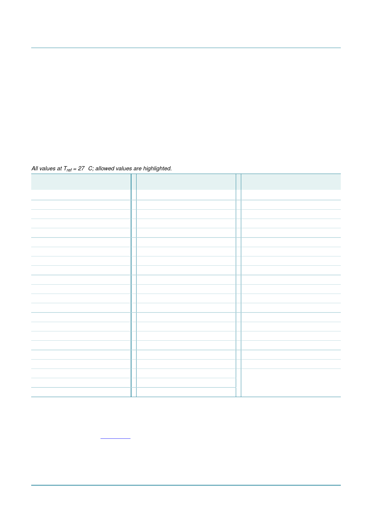
Possible values for VA and VB are between 0 to 63.
Remarks:
• Values producing more than 6.5 V at operating temperature are not allowed.
Operation above this voltage may damage the device. When programming the
operating voltage the temperature coefficient of VLCDOUT must be taken into account.
• Values below 2.2 V are below the specified operating range of the chip and are
therefore not allowed.
Table 5. Values of VA and VB and the corresponding VLCD values
All values at Tref = 27 °C; allowed values are highlighted.
Integer values Corresponding
of VA and VB value of VLCD in V
Integer values Corresponding
of VA and VB value of VLCD in V
0
VLCD switched off 22
3.58
1
1.90
23
3.66
2
1.98
24
3.74
3
2.06
25
3.82
4
2.14
26
3.90
5
2.22
27
3.98
6
2.30
28
4.06
7
2.38
29
4.14
8
2.46
30
4.22
9
2.54
31
4.30
10
2.62
32
4.38
11
2.70
33
4.46
12
2.78
34
4.54
13
2.86
35
4.62
14
2.94
36
4.70
15
3.02
37
4.78
16
3.10
38
4.86
17
3.18
39
4.94
18
3.26
40
5.02
19
3.34
41
5.10
20
3.42
42
5.18
21
3.50
43
5.26
Integer values
of VA and VB
44
45
46
47
48
49
50
51
52
53
54
55
56
57
58
59
60
61
62
63
Corresponding
value of VLCD in V
5.34
5.42
5.50
5.58
5.66
5.74
5.82
5.90
5.98
6.06
6.14
6.22
6.30
6.38
6.46
6.54
6.62
6.70
6.78
6.86
When the LCD supply voltage is generated on-chip, the VLCD pins should be decoupled to
VSS with a suitable capacitor. The generated VLCDOUT is independent of VDD and is
temperature compensated.
In Equation 2 the internal charge pump is not considered. However, if the supplied voltage
to VDD2 and VDD3 is below the required VLCD it is necessary to use the internal charge
pump. The multiplication factor has to be set such, that VDD2 and VDD3 (which are equal)
multiplied with the programmed multiplication factor exceeds the required VLCD under all
circumstances (i.e. at low temperatures and along with the temperature compensation -
PCF2119X_5
Product data sheet
Rev. 05 — 13 August 2009
© NXP B.V. 2009. All rights reserved.
9 of 79
Share Link: 