PCF2119VU-2-F2 Ver la hoja de datos (PDF) - NXP Semiconductors.
Número de pieza
componentes Descripción
Fabricante
PCF2119VU-2-F2 Datasheet PDF : 79 Pages
| |||
NXP Semiconductors
PCF2119x
LCD controllers/drivers
see Section 10.2.3.4). If still a higher multiplication factor is chosen, VLCD will not increase
(it is set by Equation 2) but the current that can be delivered will be higher. Also current
consumption increases (see Section 16.6).
When the VLCD generator and the direct mode are switched off, an external voltage may
be supplied at connected pins VLCDIN and VLCDOUT. VLCDIN and VLCDOUT may be higher or
lower than VDD2.
In direct mode (see Icon_ctl instruction, Section 10.2.3.3) the internal VLCD generator is
turned off and the VLCDOUT output voltage is directly connected to VDD2. This reduces the
current consumption depending on VDD2 value and LCD liquid properties.
The VLCD generator ensures that, as long as VDD is in the valid range (2.2 V to 4 V), the
required peak voltage VLCD = 6.5 V can be generated at any time.
8.5 LCD bias voltage generator
The intermediate bias voltages for the LCD display are also generated on-chip. This
removes the need for an external resistive bias chain and significantly reduces the system
current consumption. The optimum value of VLCD depends on the multiplex rate, the LCD
threshold voltage (Vth) and the number of bias levels. Using a 5-level bias scheme for the
1:18 multiplex rate allows VLCD < 5 V for most LCD liquids.
The intermediate bias levels for the different multiplex rates are shown in Table 6. These
bias levels are automatically set to the given values when switching to the corresponding
multiplex rate.
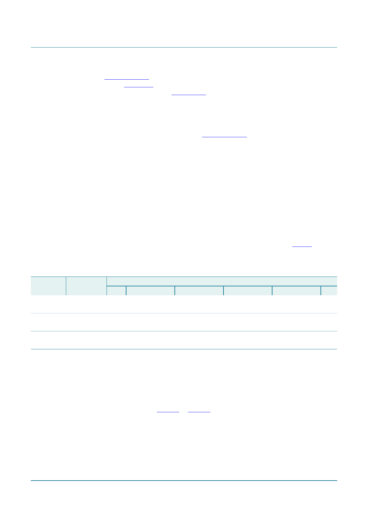
Table 6. Bias levels as a function of multiplex rate
Multiplex Number of Bias voltages
rate
bias levels
V1
V2
V3
V4
V5
V6
1:18
5
VLCD 34--(V LCD – V SS)
1--
2
(V
LCD
–
V
SS)
1--
2
(V
LCD
–
V
SS)
1--
4
(
V
LCD
–
V
S
S
)
VSS
1:9
5
VLCD 34--(V LCD – V SS)
12--(V LCD – V SS)
12--(V LCD – V SS)
14--(V LCD – V SS)
VSS
1:2
4
VLCD 23--(V LCD – V SS)
2--
3
(V
LCD
–
V
SS)
1--
3
(V
LCD
–
V
SS)
1--
3
(
V
LCD
–
V
S
S
)
VSS
8.6 LCD row and column drivers
The PCF2119x contains 18 row and 80 column drivers, which drive the appropriate LCD
bias voltages in sequence to the display in accordance with the data to be displayed. R17
and R18 drive the icon rows. Unused outputs should be left open.
The bias voltages and the timing are selected automatically when the number of lines in
the display is selected. Figure 3 to Figure 5 show typical waveforms.
PCF2119X_5
Product data sheet
Rev. 05 — 13 August 2009
© NXP B.V. 2009. All rights reserved.
10 of 79
Share Link: 